1 Product Description of DSOM-060N NXP I.MX 6ULL SOM
1.1 Product Overview and Scope
The DSOM-060N Stamp Hole System on Module is an industrial-grade embedded Linux Core Board based on NXP’s i.MX 6ULL chip(MCIMX6Y2CVM08AB ), featuring ARM’s Cortex-A7 and power management integration.
The DSOM-060 provides a variety of memory configurations, including a flexible range of DDR3L, NAND, eMMC, and SD memory cards that meet our customers’ requirements. It also supports connections to various interfaces, including two high- speed USB on-the-go with PHY, dual Ethernet, audio, display with a touch panel, and serial interfaces. In addition, the system supports industrial-grade applications targeting embedded systems.
The DSOM-060N NXP I.MX 6ULL System on Module offers a wide range of development documents and software resources that are both free and open-source. This convenience enables developers to enhance their development efficiency and shorten the development cycle.
1.2 Features
· Small and compact, measuring only 38mm x 38mm, it leads out almost all the I/O of the chip.
· EMMC capacity of 8GB, or NAND FLASH of 256MB (eMMC up to 256GB, or NAND up to 2GB optional)
· RAM 512MB LPDDR3
· Supports Linux OS ( such as Debian or Ubuntu, etc.)
· Supports 2 Ports 100M Ethernet
· Outputs 120 PIN pins with 1.2mm pitch
· CPU uses MCIMX6Y2CVM08AB, and the core module temperature range is -40 ~ 85 degrees
· RoHS certified
· The product is stable and reliable. After many high and low-temperature tests, repeated reboots, and other tests.
1.3 Application
· Industrial-embedded Linux computer
· Home Appliances
· Home Automation – Smart Home
· Human-machine Interfaces (HMI)
· Point-of-sale (POS) terminals
· Cash Register
· 2D barcode scanners and printers
· Smart grid infrastructure
· IoT gateways
· Residential gateways
· Machine vision equipment
· Robotics
· Fitness/outdoor equipment
2 System Block Diagram of DSOM-060N NXP I.MX 6ULL SOM
2.1 Main Chip Block Diagram
2.2 System on Module Block Diagram

3 Basic Parameters and Interfaces of DSOM-060N NXP I.MX 6ULL SOM
| Item | Parameter |
|---|---|
| CPU | MCIMX6Y2CVM08AB (800MHz), single-core crotexA7 , 7 92MHz |
| RAM | DDR3/ LPDDR3 standard 512M B |
| Memory | EMMC comes standard with 8 GB |
| Power Inpu | 5V/ 0.25A |
| OS | Linux( Debian, Ubuntu, .etc.) |
| Temperature | Operating Temperature: -40 °C ~85 °C |
| Storage Temperature: -50 °C ~95 °C | |
| Humidity | 10~95%(Non-condensing) |
| Barometric Pressure | 76Kpa ~106Kpa |
| Size | 38mm×38mm |
| PCB | 8 layers, immersion gold process, independent ground signal layer |
| Peripheral | Quantity | MAX Number of Channels (with multiplexing, cannot be reached simultaneously) |
|---|---|---|
| Ethernet | 2 CH | 100 Mbps Ethernet |
| UART | 8 CH | UART1 for debugging, UART3 for tutorial serial communication |
| I2C | 4 CH | One for configuring AP3216C ambient light sensor, one for configuring LCD touch |
| SPI | 4 CH | Configured for icm20608 six-axis sensor |
| CAN | 2 CH | FlexCAN1 |
| I2S | 3 CH | I2S conflicts with JTAG pins |
| 2 CH | Used for firmware burning, supporting both host and slave modes when used with the baseboard |
|
| Camera | 1 CH | supporting OV5640/2640/7725 (without FIFO) |
| JTAG | 1 CH | |
| LCD | 1 CH | RGB888 interface, supporting a maximum resolution of 1366*768 |
| ADC | 10 CH | GPIO1, can be connected to DHT11 or DS18B20 |
| PWM | 8 CH | Configured for LCD backlight |
| SDIO | 1 CH | Used for SDIO Wi-Fi or microSD card |
| GPIO | 105CH | GPIO3 is used for baseboard LEDs and can be customized with GPIO1. Additional channels can be multiplexed by modifying the device tree |
4 Pin Definition of DSOM-060N NXP I.MX 6ULL SOM
Stamp Hole eMMC Version
Back of the Stamp Hole eMMC Version
| Pin | Signal Name | Default Pin Multiplexing | Supported Pin Multiplexing | Default Function in Coreboard |
Level ( V ) | I/O Type I/O Pull |
|---|---|---|---|---|---|---|
| 1 | CSI_VSYNC | GPIO4_IO19 | CSI_VSYNC , USDHC2_CLK , I2C2_SDA , EIM_RW , GPIO4_IO19 , PWM7_OUT , UART6_RTS_B ESAI_TX4_RX1 |
CSI_VSYNC | 3.3V | |
| 2 | CSI_DATA03 | GPIO4_IO24 | CSI_DATA05 , USDHC2_DAT A3 , ECSPI2_MISO , EIM_AD03 , GPIO4_IO24 , SAI1_RX_BCLK , UART5_CTS_B , ESAI_RX_CLK |
CSI_DATA05 | 3.3V | |
| 3 | CSI_DATA07 | GPIO4_IO28 | CSI_DATA09 , USDHC2_DAT A7 , ECSPI1_MISO , EIM_AD07 , GPIO4_IO28 , SAI1_TX_DATA , USDHC1_VSEL ECT , ESAI_TX0 |
CSI_DATA09 | 3.3V | |
| 4 | CSI_DATA01 | GPIO4_IO22 | CSI_DATA03 , USDHC2_DAT A1 , ECSPI2_SS0 , EIM_AD01 , GPIO4_IO22 , SAI1_MCLK , SAI1_MCLK , ESAI_RX_HF_C LK |
CSI_DATA03 | 3.3V | |
| 5 | CSI_DATA0 | GPIO4_IO21 | CSI_DATA02 , USDHC2_DAT A0 , ECSPI2_SCLK , EIM_AD00 , GPIO4_IO21 , SRC_INT_BOO T , UART5_TX , ESAI_TX_HF_CL K |
CSI_DATA02 | 3.3V | |
| 6 | CSI_DATA04 | GPIO4_IO25 | CSI_DATA06 , USDHC2_DAT A4 , ECSPI1_SCLK , EIM_AD04 , GPIO4_IO25 , SAI1_TX_SYNC , USDHC1_WP , ESAI_TX_FS |
CSI_DATA06 | 3.3V | |
| SD1_CLK | GPIO2_IO17 | USDHC1_CLK , GPT2_COMPA RE2 , GPT2_COMPA RE2 , SPDIF_IN , EIM_ADDR20 , GPIO2_IO17 , USB_OTG1_OC |
USDHC1_CLK | 3.3V | ||
| 8 | SD1_CMD | GPIO2_IO16 | USDHC1_CMD , GPT2_COMPA RE1 , SAI2_RX_SYNC , SPDIF_OUT , EIM_ADDR19 , GPIO2_IO16 , SDMA_EXT_EV ENT00 , |
USDHC1_CMD | 3.3V | |
| USB_OTG1_PW R |
||||||
| 9 | SD1_DATA2 | GPIO2_IO20 | USDHC1_DAT A2 , GPT2_CAPTUR E1 , SAI2_RX_DATA FLEXCAN2_TX , EIM_ADDR23 , GPIO2_IO20 , CCM_CLKO1 , USB_OTG2_OC |
USDHC1_DATA 2 | 3.3V | |
| 10 | SD1_DATA3 | GPIO2_IO21 | USDHC1_DAT A3 , GPT2_CAPTUR E2 , SAI2_TX_DATA , FLEXCAN2_RX , EIM_ADDR24 , GPIO2_IO21 , CCM_CLKO2 , ANATOP_OTG 2_ID |
USDHC1_DATA 3 | 3.3V | |
| 11 | SD1_DATA1 | GPIO2_IO19 | USDHC1_DAT A1 , GPT2_CLK , SAI2_TX_BCLK , FLEXCAN1_RX , EIM_ADDR22 , GPIO2_IO19 , USB_OTG2_PW R |
USDHC1_DATA 1 | 3.3V | |
| 12 | SD1_DATA0 | GPIO2_IO18 | USDHC1_DAT A0 GPT2_COMPA |
USDHC1_DATA 0 | 3.3V | |
| RE3 , SAI2_TX_SYN , FLEXCAN1_TX , EIM_ADDR21 , GPIO2_IO18 , ANATOP_OTG 1_ID |
||||||
| 13 | SNVS_TAMP ER9 | GPIO5_IO09 | GPIO5_IO09 | GPIO5_IO09CT _RST touch reset pin |
3.3V | |
| 14 | GPIO1_IO05 | GPIO1_IO05 | ENET2_REF_CL K2 , PWM4_OUTA NATOP_OTG2_ ID , CSI_FIELD , USDHC1_VSEL ECT , GPIO1_IO05 , ENET2_1588_E VENT0_OUT , UART5_RX |
USDHC1_VSEL ECT | 3.3V | |
| 15 | LCD_ENABLE | GPIO3_IO01 | LCDIF_ENABLE , LCDIF_RD_E , UART4_RX , SAI3_TX_SYNC , EIM_CS3_B , GPIO3_IO01 , ECSPI2_RDY , EPDC_SDLE |
LCDIF_ENABE | 3.3V | |
| 16 | GPIO1_IO09 | GPIO1_IO09 | PWM2_OUT , WDOG1_WDO G_ANY , SPDIF_IN , CSI_HSYNC , USDHC2_RESE T_B , GPIO1_IO09 , USDHC1_RESE |
GPIO1_IO09 touch screen CT_INT |
3.3V | |
| T_B , UART5_CTS_B |
||||||
| 17 | GPIO1_IO04 | GPIO1_IO04 | ENET1_REF_CL K1 , PWM3_OUT , USB_OTG1_PW R , USDHC1_RESE T_B , GPIO1_IO04 , ENET2_1588_E VENT0_IN , UART5_TX |
GPIO1_IO04 | 3.3V | |
| 18 | GPIO1_IO02 | GPIO1_IO02 | I2C1_SCL , GPT1_COMPA RE2 , USB_OTG2_PW R , ENET1_REF_CL K_25M , USDHC1_WP , GPIO1_IO02 , SDMA_EXT_EV ENT00 , SRC_ANY_PU_ RESET , UART1_TX |
GPIO1_IO02 | 3.3V | |
| 19 | SNVS_TAMP ER2 | GPIO5_IO02 | GPIO5_IO05 | WIFI_INTIO is drawn but not used |
3.3V | |
| 20 | SNVS_TAMP ER5 | GPIO5_IO05 | GPIO5_IO05 | ENET1_INT_TRE EIO is drawn but not used |
3.3V | |
| 21 | SNVS_TAM PER7 | GPIO5_IO07 | GPIO5_IO07 | GPIO5_IO07 network port 1 reset pin |
3.3V | |
| 22 | SNVS_TAMP ER8 | GPIO5_IO08 | GPIO5_IO08 | GPIO5_IO08 network port 2 reset pin |
3.3V | |
| 23 | BOOT_MODE 1 |
GPIO5_IO11 | BOOT_MODE1 boot mode |
3.3V | ||
| 24 | BOOT_MODE 0 |
GPIO5_IO10 | BOOT_MODE0 boot mode |
3.3V | ||
| 25 | SNVS_TAMP ER0 |
GPIO5_IO00 | GPIO5_IO00 | GPIO5_IO00 | 3.3V | |
| 26 | SNVS_TAMP ER1 |
GPIO5_IO01 | GPIO5_IO01 | GPIO5_IO01 | 3.3V | |
| 27 | ON/OFF | SRC_RESET_B | ON/OFF | 3.3V | ||
| 28 | SNVS_TAMP ER4 |
GPIO5_IO04 | GPIO5_IO04 | GPIO5_IO04 | 3.3V | |
| 29 | 5V_IN1 | Core board power supply, input 5V |
5V | 5V _ | ||
| 30 | 5V_IN2 | Core board power supply, input 5V |
5V | 5V _ | ||
| 31 | GND | land | GND | |||
| 32 | USB_OTG2_V BUS |
USB_OTG2_V BUS |
USB powered | USB_OTG2_VB US |
3.3V | |
| 33 | USB_OTG1_V BUS |
USB_OTG1_V BUS |
USB powered | USB_OTG1_VB US |
3.3V | |
| 34 | USB_OTG2_D P |
USB_OTG2_D P |
USB_OTG2_DP | 3.3V | ||
| 35 | USB_OTG2_D N |
USB_OTG2_D N |
USB_OTG2_DN | 3.3V | ||
| 36 | USB_OTG1_D P |
USB_OTG1_D P |
USB_OTG1_DP | 3.3V | ||
| 37 | USB_OTG1_D N |
USB_OTG1_D N |
USB_OTG1_DN | 3.3V | ||
| 38 | USB_OTG1_C HD_B |
USB_OTG1_C HD_B |
USB_OTG1_CH D_B |
3.3V | ||
| 39 | GPIO1_IO00 | GPIO1_IO00 | I2C2_SCL , GPT1_CAPTUR E1 , ANATOP_OTG 1_ID , NET1_REF_CLK 1 , |
ANATOP_OTG1 _ID |
3.3V | |
| MQS_RIGHT , GPIO1_IO00 , ENET1_1588_E VENT0_IN , SRC_SYSTEM_ RESET , WDOG3_WDO G_B |
||||||
| 40 | UART1_TXD | GPIO1_IO16 | UART1_TX , ENET1_RDATA 02 , I2C3_SCL , CSI_DATA02 , GPT1_COMPA RE1 , GPIO1_IO16 , SPDIF_OUT , UART5_TX |
UART1_TX | 3.3V | |
| 41 | GPIO1_IO01 | GPIO1_IO01 | I2C2_SDA , GPT1_COMPA RE1 , USB_OTG1_OC , ENET2_REF_CL K2 , MQS_LEFT , GPIO1_IO01 , ENET1_1588_E VENT0_OUT , SRC_EARLY_RE SET , WDOG1_WDO G_B _ |
AP_INTIO is drawn but not used | 3.3V | |
| 42 | UART1_CTS_ B | GPIO1_IO18 | UART1_CTS_B , ENET1_RX_CLK , USDHC1_WP , CSI_DATA04 , ENET2_1588_E VENT1_IN , |
GPIO1_IO18 | 3.3V | |
| GPIO1_IO18 , USDHC2_WP , UART5_CTS_B |
||||||
| 43 | GPIO1_IO03 | GPIO1_IO03 | I2C1_SDA , GPT1_COMPA RE3 , USB_OTG2_OC , USDHC1_CD_B , GPIO1_IO03 , CCM_DI0_EXT_ CLK , SRC_TESTER_A CK |
GPIO1_IO03 | 3.3V | |
| 44 | UART1_RX_D ATA | GPIO1_IO17 | UART1_RX , ENET1_RDATA 03 , I2C3_SDA , CSI_DATA03 , GPT1_CLK , GPIO1_IO17 , SPDIF_IN , UART5_RX |
UART1_RX | 3.3V | |
| 45 | GPIO1_IO07 | GPIO1_IO07 | ENET1_MDC , ENET2_MDC , USB_OTG_HOS T_MODE , CSI_PIXCLK , USDHC2_CD_B , GPIO1_IO07 , CCM_STOP , UART1_RTS_B |
The two network ports of ENET1_MDC and ENET2_MDC are connected to the same IO |
3.3V | |
| 46 | GPIO1_IO06 | GPIO1_IO06 | ENET1_MDIO , ENET2_MDIO , USB_OTG_PW R_WAKE , CSI_MCLK , USDHC2_WP , GPIO1_IO06 , CCM_WAIT , |
The two network ports of ENET1_MDIO\E NET2_MDIO are connected to the same IO |
3.3V | |
| CCM_REF_EN_ B , UART1_CTS_B |
||||||
| 47 | UART1_RTS | GPIO1_IO19 | UART1_RTS_B , ENET1_TX_ER , USDHC1_CD_B , CSI_DATA05 , ENET2_1588_E VENT1_OUT , GPIO1_IO19 , USDHC2_CD_B , UART5_RTS_B |
USDHC1_CD_B | 3.3V | |
| 48 | UART2_TX_D ATA | GPIO1_IO20 | UART2_TX , ENET1_TDATA 02 , I2C4_SCL , CSI_DATA06 , GPT1_CAPTUR E1 , GPIO1_IO20 , ECSPI3_SS0 |
ECSPI3_SS0 | 3.3V | |
| 49 | UART2_RX_D ATA | GPIO1_IO21 | UART2_RX , ENET1_TDATA 03 , I2C4_SDA , CSI_DATA07 , GPT1_CAPTUR E2 , GPIO1_IO21 , SJC_DONE , ECSPI3_SCLK |
ECSPI3_SCLK | 3.3V | |
| 50 | UART2_RTS | GPIO1_IO23 | UART2_RTS_B , ENET1_COL , FLEXCAN2_RX , CSI_DATA09 , GPT1_COMPA RE3 , GPIO1_IO23 , SJC_FAIL , ECSPI3_MISO |
ECSPI3_MISO | 3.3V | |
| 51 | UART2_CTS | GPIO1_IO22 | UART2_CTS_B , ENET1_CRS , FLEXCAN2_TX , CSI_DATA08 , GPT1_COMPA RE2 , GPIO1_IO22 , SJC_DE_B , ECSPI3_MOSI |
ECSPI3_MOSI | 3.3V | |
| 52 | UART3_TX_D ATA | GPIO1_IO24 | UART3_TX , ENET2_RDATA 02 , CSI_DATA01 , UART2_CTS_B , GPIO1_IO24 , SJC_JTAG_ACT |
UART3_TX | 3.3V | |
| 53 | UART3_RX_D ATA | GPIO1_IO25 | UART3_RX , ENET2_RDATA 03 , CSI_DATA00 , UART2_RTS_B , GPIO1_IO25 , EPIT1_OUT |
UART3_RX | 3.3V | |
| 54 | UART3_CTS | GPIO1_IO26 | UART3_CTS_B , ENET2_RX_CLK , FLEXCAN1_TX , CSI_DATA10 , ENET1_1588_E VENT1_IN , GPIO1_IO26 , EPIT2_OUT |
FLEXCAN1_TX | 3.3V | |
| 55 | UART3_RTS | GPIO1_IO27 | UART3_RTS_B , ENET2_TX_ER , FLEXCAN1_RX , CSI_DATA11 , ENET1_1588_E VENT1_OUT , GPIO1_IO27 , |
FLEXCAN1_RX | 3.3V | |
| WDOG1_WDO G_B |
||||||
| 56 | UART4_RX_D ATA _ | GPIO1_IO29 | UART4_RX , ENET2_TDATA 03 , I2C1_SDA , CSI_DATA13 , CSU_CSU_ALA RM_AUT01 , GPIO1_IO29 , ECSPI2_SS0 , EPDC_PWRCTR L01 |
I2C1_SDA | 3.3V | |
| 57 | UART4_TX_D ATA | GPIO1_IO28 | UART4_TX , ENET2_TDATA 02 , I2C1_SCL , CSI_DATA12 , CSU_CSU_ALA RM_AUT02 , GPIO1_IO28 , ECSPI2_SCLK |
I2C1_SCL | 3.3V | |
| 58 | USRT5_RX_D ATA | GPIO1_IO31 | UART5_RX , ENET2_COL , I2C2_SDA , CSI_DATA15 , CSU_CSU_INT_ DEB , GPIO1_IO31 , ECSPI2_MISO , EPDC_PWRCTR L03 |
I2C2_SDA | 3.3V | |
| 59 | UART5_TX_D ATA | GPIO1_IO30 | GPIO1_IO30 , ECSPI2_MOSI , EPDC_PWRCTR L02 , UART5_TXENE T2_CRS , I2C2_SCL , CSI_DATA14 , |
I2C2_SCL | 3.3V | |
| CSU_CSU_ALA RM_AUT00 |
||||||
| 60 | ENET1_RX_E R | GPIO2_IO07 | ENET1_RX_ER , UART7_RTS_B , PWM8_OUT , CSI_DATA23 , EIM_CRE , GPIO2_IO07 , KPP_COL03 , GPT1_CAPTUR E2 , EPDC_SDOEZ |
ENET1_RX_ER | 3.3V | |
| 61 | ENET1_TX_CL K | GPIO2_IO06 | ENET1_TX_CLK , UART7_CTS_B , PWM7_OUT , CSI_DATA22 , ENET1_REF_CL K1 , GPIO2_IO06 , KPP_ROW03 , GPT1_CLK , EPDC_SDOED |
ENET1_TX_CLK | 3.3V | |
| 62 | ENET1_TX_D ATA1 | GPIO2_IO04 | ENET1_TDATA 01 , UART6_CTS_B , PWM5_OUT , CSI_DATA20 , ENET2_MDIO , GPIO2_IO04 , KPP_ROW02 , WDOG1_WDO G_RST_B_DEB , EPDC_SDCE08 |
ENET1_TDATA0 1 | 3.3V | |
| 63 | ENET1_TX_E N | GPIO2_IO05 | ENET1_TX_EN , UART6_RTS_B , PWM6_OUT , CSI_DATA21 , ENET2_MDC , |
ENET1_TX_EN | 3.3V | |
| GPIO2_IO05 , KPP_COL02 , WDOG2_WDO G_RST_B_DEB , EPDC_SDCE09 |
||||||
| 64 | EXET1_RX_D ATA0 | GPIO2_IO00 | ENET1_RDATA 00 , UART4_RTS_B , PWM1_OUT , CSI_DATA16 , FLEXCAN1_TX , GPIO2_IO00 , KPP_ROW00 , USDHC1_LCTL , EPDC_SDCE04 |
ENET1_RDATA 00 | 3.3V | |
| 65 | ENET1_RX_E N | GPIO2_IO02 | ENET1_RX_EN , UART5_RTS_B , CSI_DATA18 , FLEXCAN2_TX , GPIO2_IO02 , KPP_ROW01 , USDHC1_VSEL ECT , EPDC_SDCE06 |
ENET1_RX_EN | 3.3V | |
| 66 | ENET1_RX_D ATA1 | GPIO2_IO01 | ENET1_RDATA 01 , UART4_CTS_B , PWM2_OUT , CSI_DATA17 , FLEXCAN1_RX , GPIO2_IO01 , KPP_COL00 , USDHC2_LCTL , EPDC_SDCE05 |
ENET1_RDATA 01 | 3.3V | |
| 67 | ENET1_TX_D ATA0 | GPIO2_IO03 | ENET1_TDATA 00 , UART5_CTS_B , |
ENET1_TDATA0 0 | 3.3V | |
| CSI_DATA19 , FLEXCAN2_RX , GPIO2_IO03 , KPP_COL01 , USDHC2_VSEL ECT , EPDC_SDCE07 |
||||||
| 68 | JATG_MOD | SJC_MOD | SJC_MOD , GPT2_CLK , SPDIF_OUT , ENET1_REF_CL K_25M , CCM_PMIC_RD Y , GPIO1_IO10 , SDMA_EXT_EV ENT00 |
JATG_MODIO leads but does not use him |
3.3V | |
| 69 | JTAG TRST_ B | SJC_TRSTB | SJC_TRSTB , GPT2_COMPA RE3 , SAI2_TX_DATA , PWM8_OUT , GPIO1_IO15 , CAAM_RNG_O SC_OBS |
SAI2_TX_DATA | 3.3V | |
| 70 | JTAG_TMS | SJC_TMS | SJC_TMS , GPT2_CAPTUR E1 , SAI2_MCLK , CCM_CLKO1 , CCM_WAIT , GPIO1_IO11 , SDMA_EXT_EV ENT01 , EPIT1_OUT |
SAI2_MCLK | 3.3V | |
| 71 | JTAG_TCK | SJC_TCK | SJC_TCK , GPT2_COMPA RE2 , SAI2_RX_DATA |
SAI2_RX_DATA | 3.3V | |
| , PWM7_OUT , GPIO1_IO14 , SIM2_POWER_ FAIL |
||||||
| 72 | JTAG_TDO | SJC_TDO | SJC_TDO , GPT2_CAPTUR E2 , SAI2_TX_SYNC , CCM_CLKO2 , CCM_STOP , GPIO1_IO12 , MQS_RIGHT , EPIT2_OUT |
SAI2_TX_SYNC | 3.3V | |
| 73 | JTAG_TDI | SJC_TDI | SJC_TDI , GPT2_COMPA RE1 , SAI2_TX_BCLK , PWM6_OUT , GPIO1_IO13 , MQS_LEFT , SIM1_POWER_ FAIL |
SAI2_TX_BCLK | 3.3V | |
| 74 | GPIO1_IO08 | GPIO1_IO08 | PWM1_OUT , WDOG1_WDO G_B , SPDIF_OUT , CSI_VSYNC , USDHC2_VSEL ECT , GPIO1_IO08 , CCM_PMIC_RD Y , UART5_RTS_B |
PWM1_OUTBL T_PWM screen backlight |
3.3V | |
| 75 | LCD_CLK | GPIO3_IO00 | LCDIF_CLK , LCDIF_WR_RW N , UART4_TX , SAI3_MCLK , EIM_CS2_B , GPIO3_IO00 , |
LCDIF_CLK | 3.3V | |
| WDOG1_WDO G_RST_B_DEB , EPDC_SDCLK |
||||||
| 76 | LCD_HSYNC | GPIO3_IO02 | LCDIF_HSYNC , LCDIF_RS , UART4_CTS_B , SAI3_TX_BCLK , WDOG3_WDO G_RST_B_DEB , GPIO3_IO02 , ECSPI2_SS1 , EPDC_SDOE |
LCDIF_HSYNC | 3.3V | |
| 77 | LCD_VSYNC | GPIO3_IO03 | LCDIF_VSYNC , LCDIF_BUSY , UART4_RTS_B , SAI3_RX_DATA , WDOG2_WDO G_B , GPIO3_IO03 , ECSPI2_SS2 , EPDC_SDCE00 |
LCDIF_VSYNC | 3.3V | |
| 78 | VDD_COIN_3 V | Can do RTC function. powered by a lithium battery |
VDD_COIN_3V battery power supply |
3.3V | ||
| 79 | PMIC_ON_RE Q | Used to control the backplane 3.3V power supply |
PMIC_ON_REQ | 3.3V | ||
| 80 | RESET | chip reset pin | RESET | 3.3V | ||
| 81 | SNVS_TAMP ER6 |
GPIO5_IO06 | GPIO5_IO06 | ENET2_INT_TRE EIO is not used |
3.3V | |
| 82 | ENET2_RX_D ATA0 | GPIO2_IO08 | ENET2_RDATA 00 , UART6_TX , I2C3_SCL , |
ENET2_RDATA 01 | 3.3V | |
| ENET1_MDIO , GPIO2_IO08 , KPP_ROW04 , USB_OTG1_PW R , EPDC_SDDO08 |
||||||
| 83 | ENET2_RX_D ATA1 | GPIO2_IO09 | ENET2_RDATA 01 , UART6_RX , I2C3_SDA , ENET1_MDC , GPIO2_IO09 , KPP_COL04 , USB_OTG1_OC , EPDC_SDDO09 |
ENET2_RDATA 01 | 3.3V | |
| 84 | ENET2_TX_D ATA0 | GPIO2_IO11 | ENET2_TDATA 00 , UART7_RX , I2C4_SDA , EIM_EB_B02 , GPIO2_IO11 , KPP_COL05 , KPP_COL05 |
ENET2_TDATA0 0 | 3.3V | |
| 85 | ENET2_TX_D ATA1 | GPIO2_IO12 | ENET2_TDATA 01 , UART8_TX , ECSPI4_SCLK , EIM_EB_B03 , GPIO2_IO12 , KPP_ROW06 , USB_OTG2_PW R , EPDC_SDDO12 |
ENET2_TDATA0 1 | 3.3V | |
| 86 | ENET2_RX_E R | GPIO2_IO15 | ENET2_RX_ER , UART8_RTS_B , ECSPI4_SS0 , EIM_ADDR25 , GPIO2_IO15 , |
ENET2_RX_ER | 3.3V | |
| KPP_COL07 , WDOG1_WDO G_ANY , EPDC_SDDO15 |
||||||
| 87 | ENET2_RX_E N | GPIO2_IO10 | ENET2_RX_EN , UART7_TX , I2C4_SCL , EIM_ADDR26 , GPIO2_IO10 , KPP_ROW05 , ENET1_REF_CL K_25M , EPDC_SDDO10 |
The principle icon is ENET2_CRS_DV , but the actual name is ENET2_RX_EN |
3.3V | |
| 88 | ENET2_TX_E N | GPIO2_IO13 | ENET2_TX_EN , UART8_RX , ECSPI4_MOSI , EIM_ACLK , GPIO2_IO13 , KPP_COL06 , USB_OTG2_OC , EPDC_SDDO13 |
ENET2_TX_EN | 3.3V | |
| 89 | ENET2_TX_CL K | GPIO2_IO14 | ENET2_TX_CLK , UART8_CTS_B , ECSPI4_MISO , ENET2_REF_CL K2 , GPIO2_IO14 , KPP_ROW07 , ANATOP_OTG 2_ID , EPDC_SDDO14 |
ENET2_TX_CLK | 3.3V | |
| 90 | GND | land | GND | |||
| 91 | LCD_DATA23 | GPIO3_IO28 | EPDC_SDCE03 , LCDIF_DATA23 MQS_LEFT , MQS_LEFT , |
LCDIF_DATA23 | 3.3V | |
| CSI_DATA15 , EIM_DATA15 , GPIO3_IO28 , SRC_BT_CFG31 , USDHC2_DAT A3 |
||||||
| 92 | LCD_DATA22 | GPIO3_IO27 | LCDIF_DATA22 , MQS_RIGHT , ECSPI1_MOSI , CSI_DATA14 , EIM_DATA14 , GPIO3_IO27 , SRC_BT_CFG30 , USDHC2_DAT A2 , EPDC_SDCE02 |
LCDIF_DATA22 | 3.3V | |
| 93 | LCD_DATA21 | GPIO3_IO26 | LCDIF_DATA21 , UART8_RX , ECSPI1_SS0 , CSI_DATA13 , EIM_DATA13 , GPIO3_IO26 , SRC_BT_CFG29 , USDHC2_DAT A1 , EPDC_SDCE01 |
LCDIF_DATA21 | 3.3V | |
| 94 | LCD_DATA20 | GPIO3_IO25 | EIM_DATA12 , GPIO3_IO25 , SRC_BT_CFG28 , USDHC2_DAT A0 , EPDC_VCOM0 1 , LCDIF_DATA20 , UART8_TX , |
LCDIF_DATA20 | 3.3V | |
| ECSPI1_SCLK , CSI_DATA12 |
||||||
| 95 | LCD_DATA1 9 | GPIO3_IO24 | EIM_DATA11 , GPIO3_IO24 , SRC_BT_CFG27 , USDHC2_CLK , EPDC_VCOM0 0 , LCDIF_DATA19 , PWM6_OUT , WDOG1_WDO G_ANY , CSI_DATA11 |
LCDIF_DATA19 | 3.3V | |
| 96 | LCD_DATA18 | GPIO3_IO23 | LCDIF_DATA18 , PWM5_OUT , CA7_MX6ULL_ EVENTO , CSI_DATA10 , EIM_DATA10 , GPIO3_IO23 , SRC_BT_CFG26 , USDHC2_CMD , EPDC_BDR01 |
LCDIF_DATA18 | 3.3V | |
| 97 | LCD_DATA17 | GPIO3_IO22 | LCDIF_DATA17 , UART7_RX , CSI_DATA00 , EIM_DATA09 , GPIO3_IO22 , SRC_BT_CFG25 , USDHC2_DAT A7 , EPDC_GDSP |
LCDIF_DATA17 | 3.3V | |
| 98 | LCD_DATA16 | GPIO3_IO21 | LCDIF_DATA16 , UART7_TX , CSI_DATA01 , EIM_DATA08 , |
LCDIF_DATA16 | 3.3V | |
| GPIO3_IO21 , SRC_BT_CFG24 , USDHC2_DAT A6 , EPDC_GDCLK |
||||||
| 99 | LCD_DATA15 | GPIO3_IO20 | LCDIF_DATA15 , SAI3_TX_DATA , CSI_DATA23 , EIM_DATA07 , GPIO3_IO20 , SRC_BT_CFG15 , USDHC2_DAT A5 , EPDC_GDRL |
LCDIF_DATA15 | 3.3V | |
| 100 | LCD_DATA1 4 | GPIO3_IO19 | LCDIF_DATA14 , SAI3_RX_DATA , CSI_DATA2 , EIM_DATA0 , GPIO3_IO19 , SRC_BT_CFG14 , USDHC2_DAT A4 , EPDC_SDSHR |
LCDIF_DATA14 | 3.3V | |
| 101 | LCD_DATA13 | GPIO3_IO18 | LCDIF_DATA13 , SAI3_TX_BCLK , CSI_DATA21 , EIM_DATA05 , GPIO3_IO18 , SRC_BT_CFG13 , USDHC2_RESE T_B , EPDC_BDR00 |
LCDIF_DATA13 | 3.3V | |
| 102 | LCD_DATA12 | GPIO3_IO17 | LCDIF_DATA12 , SAI3_TX_SYNC , CSI_DATA20 , EIM_DATA04 , GPIO3_IO17 , SRC_BT_CFG12 , ECSPI1_RDY , EPDC_PWRCTR L00 |
LCDIF_DATA12 | 3.3V | |
| 103 | LCD_DATA11 | GPIO3_IO16 | LCDIF_DATA11 , SAI3_RX_BCLK , CSI_DATA19 , EIM_DATA03 , GPIO3_IO16 , SRC_BT_CFG11 , FLEXCAN2_RX , EPDC_PWRSTA T |
LCDIF_DATA11 | 3.3V | |
| 104 | LCD_DATA10 | GPIO3_IO15 | LCDIF_DATA10 , SAI3_RX_SYNC , CSI_DATA18 , EIM_DATA02 , GPIO3_IO15 , SRC_BT_CFG10 , FLEXCAN2_TX , EPDC_PWRCO M |
LCDIF_DATA10 | 3.3V | |
| 105 | LCD_DATA9 | GPIO3_IO14 _ |
LCDIF_DATA09 , SAI3_MCLK , CSI_DATA17 , EIM_DATA01 , GPIO3_IO14 , SRC_BT_CFG09 |
LCDIF_DATA09 | 3.3V | |
| , FLEXCAN1_RX , EPDC_PWRWA KE |
||||||
| 106 | LCD_DATA8 | GPIO3_IO13 | LCDIF_DATA08 , SPDIF_IN , CSI_DATA16 , EIM_DATA00 , GPIO3_IO13 , SRC_BT_CFG08 , FLEXCAN1_TX , EPDC_PWRIRQ |
LCDIF_DATA08 | 3.3V | |
| 107 | LCD_DATA7 | GPIO3_IO12 | LCDIF_DATA07 , UART7_RTS_B , ENET2_1588_E VENT3_OUT , SPDIF_EXT_CL K , GPIO3_IO12 , SRC_BT_CFG07 , ECSPI1_SS3 , EPDC_SDDO07 |
LCDIF_DATA07 | 3.3V | |
| 108 | LCD_DATA6 | GPIO3_IO11 | LCDIF_DATA06 , UART7_CTS_B , ENET2_1588_E VENT3_IN , SPDIF_LOCK , GPIO3_IO11 , SRC_BT_CFG06 , ECSPI1_SS2 , EPDC_SDDO06 |
LCDIF_DATA06 | 3.3V | |
| 109 | LCD_DATA5 | GPIO3_IO10 | LCDIF_DATA05 , UART8_RTS_B , ENET2_1588_E |
LCDIF_DATA05 | 3.3V | |
| VENT2_OUT , SPDIF_OUT , GPIO3_IO10 , SRC_BT_CFG05 , ECSPI1_SS1 , EPDC_SDDO05 |
||||||
| 110 | LCD_DATA4 | GPIO3_IO9 | LCDIF_DATA04 , UART8_CTS_B , ENET2_1588_E VENT2_IN , SPDIF_SR_CLK , GPIO3_IO09 , SRC_BT_CFG04 , SAI1_TX_DATA , EPDC_SDDO04 |
LCDIF_DATA04 | 3.3V | |
| 111 | LCD_DATA3 | GPIO3_IO8 | LCDIF_DATA03 , PWM4_OUT , ENET1_1588_E VENT3_OUT , I2C4_SCL , GPIO3_IO08 , SRC_BT_CFG03 , SAI1_RX_DATA , EPDC_SDDO03 |
LCDIF_DATA03 | 3.3V | |
| 112 | LCD_DATA2 | GPIO3_IO7 | LCDIF_DATA02 , PWM3_OUT , ENET1_1588_E VENT3_IN , I2C4_SDA , GPIO3_IO07 , SRC_BT_CFG02 , SAI1_TX_BCLK EPDC_SDDO02 |
LCDIF_DATA02 | 3.3V | |
| 113 | LCD_DATA1 | GPIO3_IO6 | LCDIF_DATA01 , PWM2_OUT , ENET1_1588_E VENT2_OUT , I2C3_SCL , GPIO3_IO06 , SRC_BT_CFG01 , SAI1_TX_SYNC , EPDC_SDDO01 |
LCDIF_DATA01 | 3.3V | |
| 114 | LCD_DATA0 | GPIO3_IO5 | LCDIF_DATA00 , PWM1_OUT , ENET1_1588_E VENT2_IN , I2C3_SDA , GPIO3_IO05 , SRC_BT_CFG00 , SAI1_MCLK , EPDC_SDDO00 |
LCDIF_DATA00 | 3.3V | |
| 115 | CSI_DATA5 | GPIO4_IO26 | CSI_DATA07 , USDHC2_DAT A5 , ECSPI1_SS0 , EIM_AD05 , GPIO4_IO26 , SAI1_TX_BCLK , USDHC1_CD_B , ESAI_TX_CLK |
CSI_DATA07 | 3.3V | |
| 116 | CSI_PIXCLK | GPIO4_IO18 | CSI_PIXCLK , USDHC2_WP , RAWNAND_CE 3_B , I2C1_SCL , EIM_OE , GPIO4_IO18 , SNVS_HP_VIO_ |
CSI_PIXCLK | 3.3V | |
| 5 , UART6_RX , ESAI_TX2_RX3 |
||||||
| 117 | CSI_DATA06 | GPIO4_IO27 | CSI_DATA08 , USDHC2_DAT A6 , ECSPI1_MOSI , EIM_AD06 , GPIO4_IO27 , SAI1_RX_DATA , USDHC1_RESE T_B , ESAI_TX5_RX0 |
CSI_DATA08 | 3.3V | |
| 118 | CSI_DATA02 | GPIO4_IO23 | CSI_DATA04 , USDHC2_DAT A2 , ECSPI2_MOSI , EIM_AD02 , GPIO4_IO23 , SAI1_RX_SYNC , UART5_RTS_B , ESAI_RX_FS |
CSI_DATA04 | 3.3V | |
| 119 | CSI_MCLK | GPIO4_IO17 | CSI_MCLK , USDHC2_CD_B , RAWNAND_CE 2_B , I2C1_SDA , EIM_CS0_B , GPIO4_IO17 , SNVS_HP_VIO_ 5_CTL , UART6_TX , ESAI_TX3_RX2 |
CSI_MCLK | 3.3V | |
| 120 | CSI_HSYNC | GPIO4_IO20 | CSI_HSYNC , USDHC2_CMD , I2C2_SC , EIM_LBA_B , |
CSI_HSYNC | 3.3V | |
| GPIO4_IO20 , PWM8_OUT , UART6_CTS_B , ESAI_TX1 |
5 Electrical Parameters of DSOM-060N NXP I.MX 6ULL SOM
5.1 Absolute Electrical Parameters
| Parameter | Description | Min Value |
Max Value |
unit | |||
|---|---|---|---|---|---|---|---|
| 5V_IN( _1/_2 ) | 5V_IN( _1/_2 ) Input voltage | -0.3 | 6.0 _ | V | |||
| VDD_COIN_3V | RTC power input | -0.3 | 3.6 _ | V | |||
| Ta | Operating temperature range | -40 | 85 | ℃ | |||
| Ts | Store temperature range | -50 | 95 | ℃ | |||
Note: Exposure to conditions beyond the absolute maximum ratings may cause permanent damage and affect the reliability and safety of the device and its systems. The functional operations cannot be guaranteed beyond specified values in the recommended conditions.
5.2 Normal working parameters
| Parameter | Description | Min Value | Typical Value |
Max Value | Unit | |||
|---|---|---|---|---|---|---|---|---|
| 5V_IN( _1/_2 ) | 5V_IN( _1/_2 ) Input voltage | 4.8 | 5 | 5.2 | V | |||
| VDD_COIN_3V | RTC power input | 2.9 | 3.0 | 3.3 | V | |||
| 5V_IN( _1/_2 ) Supply Current | 5V_IN( _1/_2 ) Input current | 0.3 | A | |||||
| Ta | Operating temperature range | -40 | 25 | 85 | ℃ | |||
| Ts | Store temperature range | -50 | 25 | 95 | ℃ | |||
6 Hardware Design Guidelines of DSOM-060N NXP I.MX 6ULL SOM
6.1 System Boot Configuration
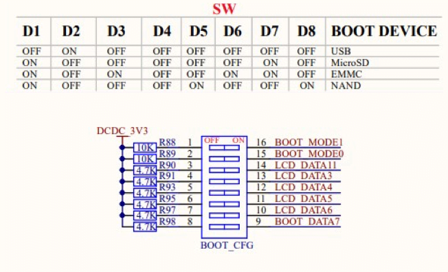
The firmware for the system on module is stored on an external storage device such as an
EMMC, NAND, or SD card. To boot correctly, the System on Module requires a boot
configuration that allows it to read the firmware from the correct memory location.
The boot configuration design can be found on the development board.
An eight-position dip switch can be used to accommodate the need for four-mode
configurations. In addition, the 3.3V power supply used here provides all the power
for the peripherals on the carrier board.
6.6 Debugging the Serial Port
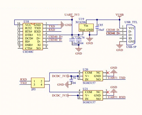
The development board connects the CH340 to the debug serial port for easy
debugging and adds an analogue switch for isolation between the two. The purpose
of the analogue switch is to prevent the CH340 from interfering with the startup of
the system on module via the pins of the debug serial port. When creating your own
backplane, you can design it according to your actual situation.
6.7 Network Port
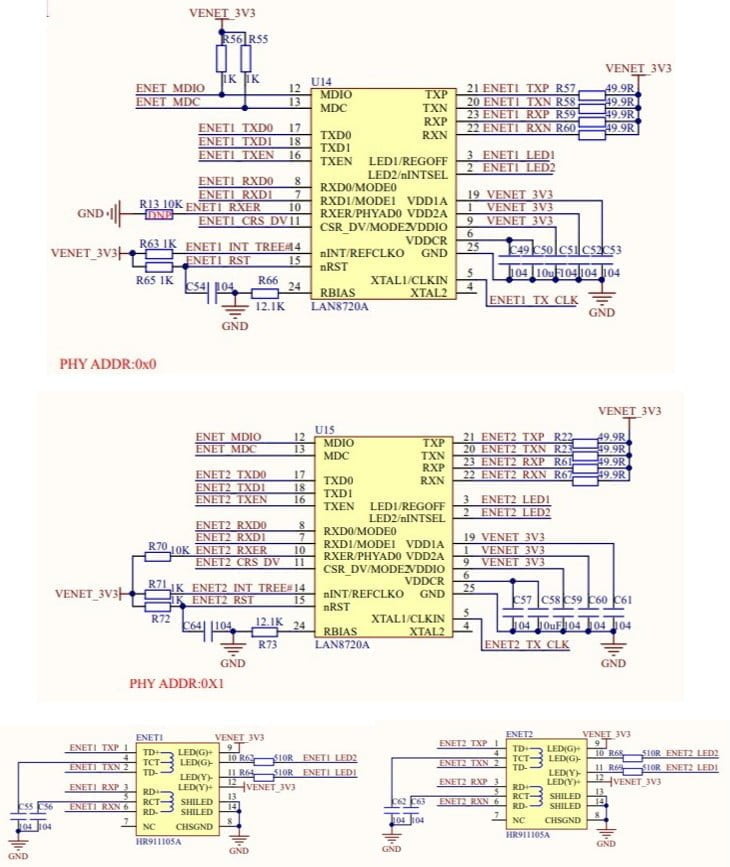
Note: the wiring between the PHY chip and the system on module should not be too long,
and try to keep the PHY chip as close to the System on Module as possible. As the core
board will provide 50MHz clock to the PHY chip through one pin, the wiring of this
pin is too long, which will lead to poor signal quality, and the PHY will not be
recognized properly. The core board manages and communicates with the PHY chip
via two pins, MDIO and MDC, and the data is transmitted via the TX and RX related
pins. The data lines between the PHY chip and the network interface need to be
differential. The alignment should ideally meet the requirements of the relevant
alignment standards.
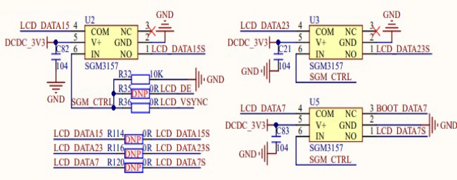
6.8 RGB-LCD Pins
The LCD_DATA pin is both a data pin for connecting to the LCD screen and a boot
configuration pin at boot time. When the LCD screen is not in use, this part of the
pin can be reused for other functions, but it should be noted that the connected
external device will not set this part of the pin high or low when it is powered up to
avoid interfering with the level state read by the core board during boot time. If the
correct level is not read, the System on Module will not be able to load the Linux firmware
correctly from the external storage and boot.
In the development board, our screen uses three LCD_DATA pins as screen ID pins,
and there are soldered pull-up and pull-down resistors on the ID pins. As the
soldered pull-up and pull-down resistors will affect the normal startup of the
development board, the development board adds three analog switches to the LCD
interface for isolation. The following diagram shows.
6.9 PIO5 (GPIO1-05)
The GPIO5 pinout on the system on module requires attention when in use. This pin is used
to switch the voltage of the SDIO1 interface. When GPIO5 is high, it sets the logic
high level of the SDIO1 interface to 1.8V. When low, it sets the logic high level to
3.3V. Note that when using the SDIO1 interface pin, the GPIO5 pin level should
remain unchanged to avoid voltage changes causing peripheral and core board
logic levels to be incompatible, which can result in abnormal operation. When using the GPIO5 and SDIO1 interfaces, ensure that the peripheral connected to the SDIO1
interface is compatible with both voltage levels. Otherwise, it is recommended to
leave GPIO5 vacant and use only the SDIO1 interface.
6.10 RTC section
6.11 PMIC_ON_REQ pin
6.12 Core board start-up problems
· The System on Module (SOM) will not boot properly with a direct 5V supply. An appropriate
boot circuit on the carrier board is required for the core board to boot correctly.
· If the boot circuit is present, the power-up timing must be followed. The core
board first receives a 5V supply, and after it has stabilised, PMIC_ON_REQ is
pulled up to enable the 3.3V output of the base board via PMIC_ON_REQ, and
3.3V pulls up the configuration pins for booting. The core board reads the
configuration pins and starts the firmware in the appropriate memory.
· The core board has specific requirements for 5V and 3.3V. Some of the DC-DC
voltage conversion chips require a small rise time to stabilise the 5V output
after enabling. The 5V and 3.3V rise time should be as short as possible, and
the 3.3V used by the peripherals on the base board should preferably be output
after the 3.3V is enabled. As soon as PMIC_ON_REQ is pulled high, it reads the
configuration information from the pull switch. The specific time for this is not
disclosed by NXP. We have tested that there is no extra time, basically
PMIC_ON_REQ is pulled high and then reads the startup configuration. If it does
not read it or reads the wrong configuration, it will not start or will go into false
death.
· To determine if the core board is in the shutdown state, measure the voltage
on the core board. If the core board is operating normally, the ON_OFF pin and
the PMIC_ON_REQ pin will output a high level. In the shutdown state, the
ON_OFF pin remains high and PMIC_ON_REQ becomes low. To exit the
shutdown state, time-delay the ON_OFF pin to ground and wait for
PMIC_ON_REQ to return to a high level.
· Power-up of the peripherals on the carrier board must follow the power-up of
the core board, otherwise current backflow will occur, preventing normal
startup of the core board.
6.13 Some Peripheral Interface Problems
· If a USB device keeps asking for a new device or does not respond when connected,
check that the USB_OTG_VBUS power supply to the System on Module is normal, that the
power supply to the USB interface is normal (USB devices must be powered from
the female connector) and that the orientation of the USB data cable conforms to
the orientation standard.
· If the TF card does not respond or initialization fails, ground the shell of some TF
cardholders to make the TF card work properly. To ensure smooth data transfer,
check that the power supply and data cable alignment complies with the SDIO
alignment standard. The PHY chip and the core board should not be too far apart.
Try to keep the PHY chip and core board close together to avoid degradation of
communication quality caused by long alignment. Alignments should be as close
to the standard as possible.
7 Product Dimensions of DSOM-060N NXP I.MX 6ULL SOM
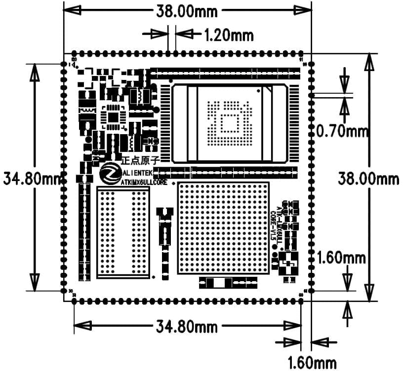

| Item | Parameter |
|---|---|
| Exterior | Stamp Hole |
| Core Board Size | 38mm*38mm |
| Pin Spacing | 1.2mm |
| Pin Pad Size | 2.0mm*0.7mm |
| Number of Pins | 120 Pins |
| Number of Layers | 8 floors |
| Warpage | less than 0.5 % |
Documentations
DusunIoT offers full set of development resources including QUICK START, SDK, Firmware packaging, module firmware, Tools, vairous third party software,etc.