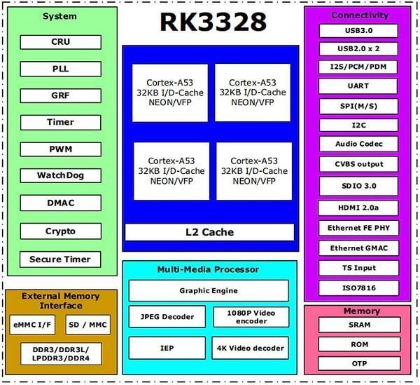
1. DSOM-010R RK3328 SoM Introduction
DSOM-010R RK3328 SoM uses the Rockchip RK3328 Cortex-A53 quad-core processor and runs Android/Linux+QT/Ubuntu OS with a high-performance frequency of 1.5GHz. It features the Mali450MP2 GPU, supporting 4K video encoding and H.264 hardware decoding.
RK3328 system on module has rich interfaces, with all function pins available for external device expansion, making it an ideal choice for human-computer interaction and industrial automation projects.
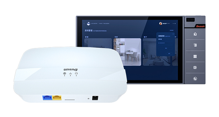
This system on module is also a versatile Android-based intelligent core board, widely used in products such as facial recognition devices, smart display terminals, video terminals, and industrial automation terminals, including advertising machines, digital signboards, smart self-service terminals, smart retail terminals, smart homes, O2O smart devices, industrial control hosts, and robot devices, among others.
The DSOM-010R SoM offers a wide range of development documents and software
resources that are both free and open-source. This convenience enables developers to enhance their efficiency and shorten the development cycle.
- Featuring a compact form factor and sufficient GPIO interfaces
- Size 44mm*44mm
- Utilizes RK805 PMU ensuring stable and reliable operation
- eMMC up to 32GB
- RAM up to 2GB
- Stamp hole soldering core board, with built-in CVBS and HDMI
- Supports customization of Android/Linux+QT system, providing system call interface API reference code and enabling perfect support for customer upper-level application APP development and SDK
- Supports 100M/1000M Ethernet;
- Leads out 132 PIN pins, including all CPU pins.
- Size 44mm*44mm
- RoHS certified
- IoT gateways
- Robotics
- Facial recognition devices
- Smart display terminals
- Video terminals
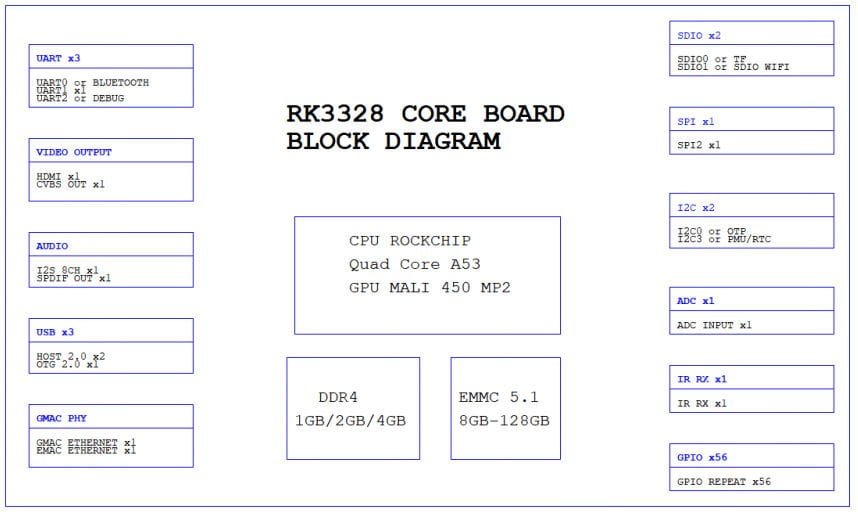
2. DSOM-010R RK3328 SoM System Block Diagram
3. Basic Parameters and Interfaces of DSOM-010R RK3328 SOM
| Item | Parameter |
|---|---|
| CPU | Quad-Core ARM® Cortex-A53 64-bit processor, Frequency up to 1.5GHz |
| GPU | ARM Mali-450 MP2 Quad-Core GPU Support OpenGL ES1.1/2.0, OpenVG1.1 Frequency up to 500 MHz |
| VPU | Support 4K VP9 and 4K 10bits H265 / H264 video decoding, up to 60fps 1080P multi-format video decoding (WMV, MPEG-1/2/4, VP9, H.264, H.265) 1080P video coding, support H.264/H.265 Video postprocessor: de-interlacing, denoising, edge/detail/color optimization |
| RAM | 2GB (1GB optional) |
| Storage | eMMC 32 GB (8GB / 16GB / 32GB / 64G / 128G eMMC optional) |
| Power Management | RK805-1 |
| Operating Voltage | Typical voltage 5V/2A |
| OS | Android, Debian |
| Temperature | Operating Temperature: 0 °C ~80 °C |
| Storage Temperature: -40 °C ~85 °C | |
| Humidity | 10~95% (Non-condensing) |
| Barometric Pressure | 76Kpa ~106Kpa |
| Size | 44mm x 44mm x 3.0mm |
| Item | Parameter |
|---|---|
| Ethernet | Integrated GMAC Ethernet controller extended 1×10/100Mbps Ethernet or 1×10/100/1000Mbps Ethernet |
| HDMI | support maximum 4K/1080P display |
| CVBS | Support CVBS output |
| UART | 3-way serial port, one of which is for debugging |
| I2C | 2-way I2C |
| I2S | 1 x I2S with 8 channel |
| SDIO | 1 x SDIO for Wi-Fi AP6212 |
| SPI | 1 x SPI |
| USB 2.0 | 2 x USB2.0, one of which is for OTG |
| USB 3.0 | 1 x USB3.0 |
| TF | 1 x TF |
| GPIO | Defined features |
| ADC | 1 x ADC |
| Upgrade | supports local firmware upgrades via USB interface |
4. Pin Definition of DSOM-010R RK3328 SOM
| Pin | Name | I/O Type | I/O Def | I/O Voltage (High/Low) | I/O Driver (Unit:mA) | I/O Voltage (Unit:V) | Feature |
|---|---|---|---|---|---|---|---|
| 1 | USB30_TXP | O | O | USB30_TXP | |||
| 2 | USB30_TXN | O | O | USB30_TXN | |||
| 3 | USB30_RXP | I | I | USB30_RXP | |||
| 4 | USB30_RXN | I | I | USB30_RXN | |||
| 5 | USB30_DP | I/O | I | USB30_DP | |||
| 6 | USB30_DM | I/O | I | USB30_DM | |||
| 7 | GND | P | 0 | GND | |||
| 8 | AOL | O | O | AOL | |||
| 9 | AOR | O | O | AOR | |||
| 10 | GND | P | 0 | Ground | |||
| 11 | VDAC_OUT | O | O | VDAC_OUT | |||
| 12 | GND | P | 0 | GND | |||
| 13 | GPIO0_A2 | I/O | I | down | 4 | 3.3 | GPIO0_A2/ CLKOUT_GMAC_M0/ SPDIF_TX_M2_d |
| 14 | MUTE_CTL | O | O | 3.3 | GPIO_MUTE_d | ||
| 15 | GPIO0_A0 | I/O | I | down | 4 | 3.3 | GPIO0_A0/ CLKOUT_WIFI_M0_d |
| ... | |||||||
NOTE:
I/O types: I = digital-input, O = digital-output, I/O = digital input/output (bidirectional),
A=Analog IO. Def default IO direction for digital IO.
All GPIO pins support interrupts. P = power supply.
5. Electrical Parameters of DSOM-010R RK3328 SOM
| Parameter | Description | Min | Typ | Max | Unit |
|---|---|---|---|---|---|
| VCC_SYS | Input Voltage | -0.3 | 6.5 | V | |
| Ta | Operating temperature range | 0 | 80 | ℃ | |
| Ts | Store temperature range | -40 | 85 | ℃ |
Note: Exposure to conditions beyond the absolute maximum ratings may cause permanent damage and affect the reliability and safety of the som and its systems. The functional operations cannot be guaranteed beyond specified values in the recommended conditions.
| Parameter | Description | Min | Typ | Max | Unit |
|---|---|---|---|---|---|
| VCC_SYS | Input Voltage | 4.75 | 5 | 5.25 | V |
| Ta | Operating temperature range | -20 | 25 | 60 | ℃ |
| Ts | Store temperature range | -20 | 25 | 70 | ℃ |
| Current (Without any other peripherals connected ) | Startup current | 370 | 576 | 1023 | mA |
| Static current | 360 | mA |
6. Hardware Design Guidelines of DSOM-010R RK3328 SOM
The RK3328 provides two SDMMC interface controllers supporting the SDMMC 3.0 protocol. However, the current System on Module is not designed for 1.8V/3.3V power switching, so it only supports the SDMMC 2.0 protocol.
- SDMMC0 is multiplexed with UART2 and JTAG functions.
- The SDMMC0EXT controller also supports the SDMMC 3.0 protocol, but due to power design limitations, it only supports SDIO 2.0. It can be used to connect to TF cards or SDIO WIFI
The recommended pull-up/down and matching design for the SDMMC interface are as follows:
| Signal | Internal pullpull-upn | Connection method | Description |
|---|---|---|---|
| SDMMC_DQ[3:0] | Pull-up | Series with 22ohm resistor | SD data transmission/ reception |
| SDMMC_CLK | Pull-down | Series with 22ohm resistor | SD clock transmission |
| SDMMC_CMD | Pull-up | Series with 22ohm resistor | SD command transmission/ reception |
In order to meet the requirements of ESD protection, it is necessary to consider designing protection circuits on the SDMMC circuit in circuit design. To avoid the impact of protection devices on SDMMC signals and achieve good protection effect, the following principles are recommended for PCB design:
- The protection device is recommended to be placed close to the SDMMC connector port.
- It is recommended that the parasitic capacitance of the protection device be less than 10pF.
SDIO/SDMMC PCB design routing should pay attention to the following:
- CLK should be routed separately and have ground shielding
- DATA lines should follow the 3W rule for spacing
- TF card only supports up to SDMMC2.0 and has no separate power supply, while Wi-Fi supports up to SDIO3.0 and a clock frequency of up to 180MHz.
Therefore, SDIO_D0/1/2/3, SDIO_CLK, and SDIO_CMD should be routed carefully on the PCB layout to avoid interference and ensure consistency.
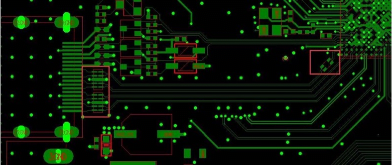
The highlighted yellow part in the diagram below is the SDIO routing, and the PCB routing should maintain the integrity of the reference layer (adjacent layers should maintain the same plane) to avoid interference from other signals,s such aspowereTheee lines on the same layer should be isolated with GND.
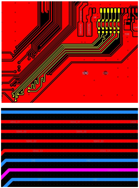
- Due to the long length of the tracks, the spacing between them is recommended to be 8mil.
- The load capacitance consists of two parts: the SD card load’s capacitance and the PCB load’s capacitance. The load capacitance for the SD card should be less than 10pF according to the protocol requirements.
| Parameters | Requirement |
|---|---|
| 3.0V Operation | 50 MHz with 40 pF |
| 1.8V Operation | 208 MHz with 21 pF |
| Capacitance | Min | Max | Units | Notes |
|---|---|---|---|---|
| CCARD (CDIE + CPKG) | 5 | 10 | pF | --- |
| Parameters | Requirement |
|---|---|
| Trace Impedance | 50Ω±10% single ended |
| Max skew between data signal and clock | <20ps |
| Max trace length | <3.93 in |

Wi-Fi communicates with the RK3328 chip through either SDIO or USB, while Bluetooth communicates with the RK3328 chip through UART or PCM interface. For SDIO PCB design, please refer to the design considerations for SDIO in section 3.3.1. Bluetooth communicates with the RK3328 chip through UART (up to 4Mbps), and the PCB layout for UART should also maintain the integrity of the reference layer as much as possible.
For the PCB layout of I2S/PCM, the adjacent reference layers should be kept intact (the adjacent layers should be in the same plane) to avoid interference from other signals s,uch as power, and the lines should be isolated from GND on the same layer.

The RK3328 integrates a Gigabit Ethernet MAC and a 100Mbps Ethernet PHY internally and can be used with an external Gigabit Ethernet PHY to achieve Gigabit network functionality. It can also use the integrated 100Mbps Ethernet PHY to achieve 100Mbps network functionality. Simultaneously using both can achieve dual-port (Gigabit + 100Mbps) functionality. For specific design information regarding Gigabit Ethernet, please refer to the design documentation provided by the PHY manufacturer. The working clock for the PHY can be selected from an external crystal or provided by the MAC_CLK output of the RK3328 chip.
The RK3328 supports 10/100/1000M MAC. The design and precautions for the 1000M GMAC are described below.
| Signal | Internalpull upp/down | Connection method | Description |
|---|---|---|---|
| MAC_TXCLK | Pull-down | Series 22 ohm resistor | Reference clock for data transmission |
| MAC_RXCLK | Pull-down | Series 22 ohm resistor | Reference clock for data reception |
| MAC_TXD[3:0] | Pull-down | Series 22 ohm resistor | Data transmission |
| MAC_RXD[3:0] | Pull-down | Series 22 ohm resistor | Data reception |
| MAC_TXEN | Pull-down | Series 22 ohm resistor | Enable data transmission |
| MAC_RXDV | Pull-down | Direct connection | Data reception valid indicator |
| MAC_MDC | Pull-down | Direct connection | Configure interface clock |
| MAC_MDIO | Pull-down | Direct connection | Configure interface I/O |
| MAC_CLK | Pull-down | Series 22 ohm resistor | MAC master clock output |
Power supply: The RK3328 GMAC IO voltage is 3.3V/1.8V (selected via Pin 105 on the core board), and the Ethernet PHY IO voltage needs to be consistent with the GMAC IO level.
On the RGMII interface transmission and reception signal lines, TX_CLK and RX_CLK are 125MHz. In order to achieve a transmission rate of 1000Mb, the TXD and RXD signal lines are sampled on both edges of the clock, and the data enable signals (MAC_TXEN, MAC_RXDV) must be enabled before the data is sent.
Reset: The MAC controls the reset of the PHY through GPIO, but if the IO of the PHY is 1.8V, the following circuit needs to be added.
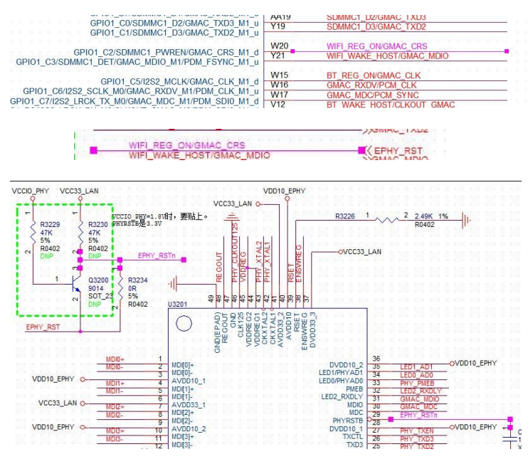
The control and status information transfer between the MAC layer and PHY is carried out through the MDIO interface, using the clock signal MDC and the data signal MDIO. It is important to note that the MDIO signal requires a pull-up resistor, and the TX signal also requires an additional pull-up resistor, as shown in the diagram below:
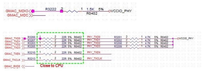
RK3328 supports built-in integration of 10/100 PHY. The PHY interface design of RK3328 includes the following:
| Signal | Internalpull upp/down | Connection method | Description |
|---|---|---|---|
| FEPHY_TXP | NA | Connect a 10 ohm resistor in series with a network transformer. | Differential signaling for data transmission |
| FEPHY_TXP | NA | Connect a 10 ohm resistor in series with a network transformer. | |
| FEPHY_TXP | NA | Connect a 10 ohm resistor in series with a network transformer. | Differential signaling for data reception |
| FEPHY_TXP | NA | Connect a 10 ohm resistor in series with a network transformer. |
When using internal 100Mbps, it is essential to note that the 10ohm resistor connected in series with the signal cannot be removed or its parameters changed.
The pull-up resistor for the differential signal should be connected to the network transformer rather than the chip.
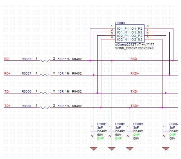
To meet the requirements of ESD protection and surge protection, it is necessary to add protection circuits in circuit design. In order to avoid the impact of protection devices on PHY wiring signals and achieve good protection effects, the following principles must be followed in PCB design:
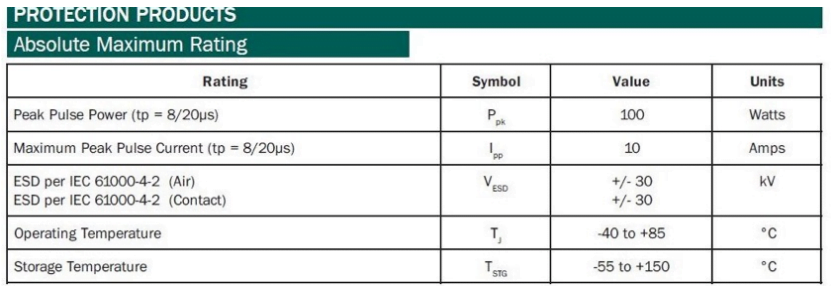
It is recommended to place the protection device on the inside of the transformer, between the transformer and the PHY, close to the transformer. Differential mode and ESD can be solved by using components. TVS tubes with a breakdown voltage of 8kV and a response time of less than 1ns are recommended for protection devices.
The cost of an integrated differential mode surge protection device may be higher compared to using individual ESD components. However, ESD components with specifications reaching the following levels can be selected instead.
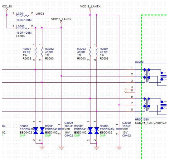
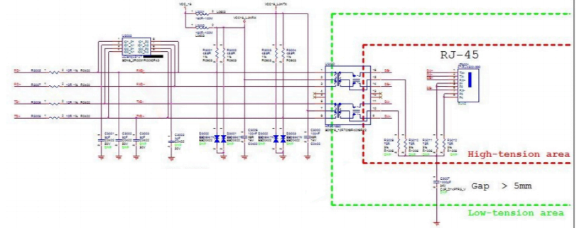
Common mode protection can be achieved through isolation spacing and AC isolation voltage provided by a network transformer. In order to meet the surge design requirements, the PCB design must ensure sufficient isolation spacing and include isolation slots. For example, if the common mode standard requires 4KV, the wires and components connected to the RJ45 connector must ensure an isolation spacing of 120 mils or more with respect to GND and the secondary of the transformer. The AC isolation voltage of the transformer itself must be in the range of 2.5-3KV or higher. If the common mode standard requires 6KV, the wires and components connected to the RJ45 connector must ensure an isolation spacing of 220 mils or more with respect to GND and the secondary of the transformer. The AC isolation voltage of the transformer itself must be in the range of 5KV or higher.
PCB design considerations:
- The closer the gigabit PHY is to RK3328, the better the effect will be. The RGMII routing should be kept below 15cm to achieve better EMI performance.
- MAC_RXCLK should be grounded.
- The series resistor of MAC_RX should be placed closer to the PHY.
- The routing of RXD[0:3], RXCLK, and RXDV should be equal in length, with a difference of less than 100mil throughout the entire length, and the routing should be as short as possible, with the entire length less than 15cm.
- There must be a complete reference plane, and other signal lines should not be routed parallel to it.
- The series-matching resistor of PHYTX should be placed close to RK3328, and PHY_TXCLK should be grounded.
- The routing of TXD[0:3], TXCLK, and TXEN should be equal in length, with a difference of less than 100mil throughout the entire length, and the routing should be as short as possible, with the entire length less than 15cm.
There must be a complete reference plane, and other signal lines should not be routed parallel to it. R3211 in the figure below should be placed closer to the PHY, grounded, and the routing should be as short as possible with a complete reference plane

The RK3328 has 2 USB 2.0 interfaces and 1 USB 3.0 interface. The recommended pull-up/pull-down and matching designs for the USB 2.0 interfaces are shown in the table below.
| Signal | Connection method | Description |
|---|---|---|
| USB0_DP/DM | Series 2.2 ohm resistor | USB2.0 HOST0&OTG Input/Output |
| USB1_DP/DM | Series 2.2 ohm resistor | USB2.0 HOST1 Input/Output |
The recommended pull-up/pull-down and matching designs for the USB 3.0 interfaces are shown in the table below.
| Signal | Connection method | Description |
|---|---|---|
| USB30_TXP/TXN | Series 0 ohm resistor | USB 3.0 Output |
| USB30_RXP/RXN | Series 0 ohm resistor | USB 3.0 Input |
| USB30_DP/DM | Series 2.2 ohm resistor | Compatible with USB 2.0, USB 2.0 HOST input/output |
USB0 serves as the system firmware burning port and cannot be adjusted arbitrarily; OTG and HOST ports can be used independently.
VBUS serves as the USB OTG insertion detection, and the input detection voltage must be less than 3.3V, and there must be a high level for the computer to recognize it, so it cannot be left unconnected.
The USB controller reference resistor should be selected with 1% accuracy, as this resistor affects the USB amplitude and eye diagram quality.
To suppress electromagnetic radiation, consider reserving a common-mode inductor (common-mode choke) on the signal line. During debugging, choose to use a resistor or a common-mode inductor based on actual conditions.
To meet ESD protection level requirements, protection circuits need to be designed in the USB circuit during circuit design. To avoid the impact of protection devices on USB wiring signals and achieve good protection effects, it is recommended to follow these principles during PCB design:
ESD protection devices should be placed close to the USB connector port.
ESD protection devices should be selected with an air discharge of 15kV, a contact discharge of 8kV, and a response time of less than 1ns.
USB 2.0 has a transmission speed of 480Mbps, so differential signals are very sensitive to parasitic capacitance on the line. Therefore, ESD protection devices with low parasitic capacitance should be selected, and the capacitance should be less than 1pF.
USB 3.0 has a transmission speed of 5Gbps, so differential signals are very sensitive to parasitic capacitance on the line. Therefore, ESD protection devices with low parasitic capacitance should be selected, and the capacitance should be less than 0.4pF.
The 2.2ohm resistor in series with the USB signal cannot have its parameters modified or omitted.
USB PCB layout considerations are as follows:
USB differential signals must be strictly routed according to differential requirements, corners cannot be right angles or sharp angles, and impedance requirements must be Z = 90±10ohm
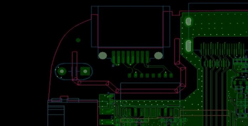
The current defined by the USB 2.0 specification is 500mA, but the VBUS trace should preferably be able to withstand a current of 1A to prevent overcurrent and reduce line loss caused by PCB layout. The USB 3.0 specification defines a current of 900mA, but the VBUS trace should preferably be able to withstand a current of 1.5A to prevent overcurrent and reduce line loss caused by PCB layout. ESD protection devices, standard mode chokes, and large capacitors should be placed as close as possible to the USB interface, current limiting switch input, and output pins. Using multiple holes to reduce trace impedance and meet overload capacity is recommended if there are holes for changing layers. Also, ensure that the ground pins of the current limiting switch have a good grounding, and place at least four 0402-type through-holes on nearby pins, as shown in the figure below:

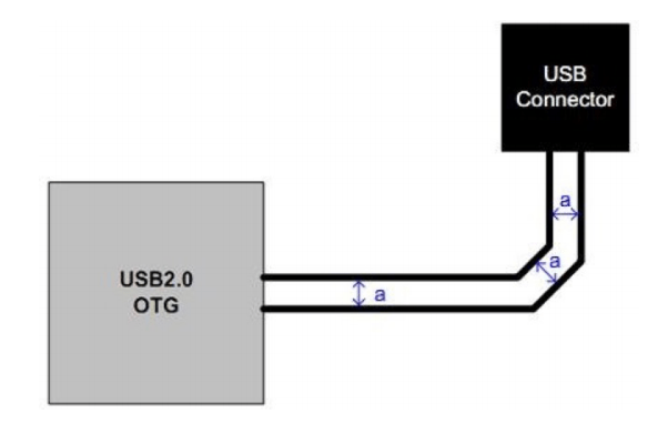
In DM/DP routing, it is advisable to minimize the use of vias, as vias can cause impedance discontinuity in the signal path. If vias must be used for layer changes, add a ground via at the center of the differential pair to provide a short signal return path. For USB routing, it is recommended to use surface routing and ensure that the routing reference plane is a continuous and uninterrupted plane, as shown in the diagram below:
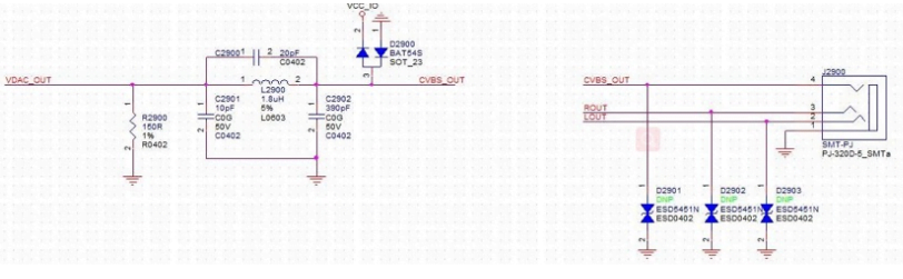
To meet standard requirements for audio, an audio amplifier IC needs to be added. The VDAC_OUT network has a lower resistance of 150 ohms, which cannot be changed, as shown in the diagram below:

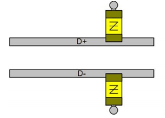
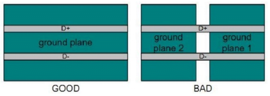
For CVBS video signals, a 75-ohm impedance control should be implemented, and PCB wiring should be kept as short as possible while avoiding interference signals such as PWM and DC-DC power inductors, especially the 12V to 5V DC-DC inductor, with a distance of at least 5mm. Additionally, the system power supply should not be used as a reference layer; the GND layer should be used instead. The ground-to-ground spacing within the same layer should be at least 2W to avoid affecting chroma and luminance gain unevenly.
For analog audio signals, the left and right channels should be grounded appropriately, and ground vias should be placed strategically to avoid strong interference from power supplies, clocks, and other signals. It is essential to avoid interference sources for digital audio signals such as SPDIF. If using coaxial cables, isolation circuits should be added to prevent equipment levels from mismatching and damaging the SPDIF IO output port. The coaxial circuit is shown in the figure below.

The RK3328 provides an HDMI interface that supports the HDMI 2.0a protocol.
When designing the HDMI interface circuit, it is essential to prevent reverse current flow. Refer to the diagram below for the design:
Refer to the diagram below for the design of the I2C bus circuit for the RK3328:

ESD protection is required for the four differential signals in HDMI. The ESD protection devices should be placed near the HDMI interface, and the recommended maximum capacitance is 0.4pF. Refer to the diagram below for the design:

- The differential signals of HDMI must strictly follow the differential requirements for wiring, and the number of layer changes should be minimized to maintain the integrity of the reference plane. The impedance requirement is Z=100±10ohm.
- The HDMI signal of RK3328 can be directly fanned out to the HDMI connector in sequence. The number of via changes should be minimized to avoid the discontinuity of the line impedance. If layer changes cannot be avoided due to mold structure, it is recommended to control the impedance change of the layer change within 10% and arrange a nearby GND near signal return at each differential pair adjacent to the layer change.
| Parameter | Requirement |
|---|---|
| Trace Impedance | Differential impedance:100Ω±10% |
| Max intra-pair skew | <4ps |
| Max trace length skew between clock and data pairs | <80ps |
| Max trace length on carrier board | 9.8inchess |
| Minimumpair-to-pairpaircing | 3 times the width of the trace. Try to increase/Spacing between pairs whenever it is possible. |
| The minimum spacing between HDMI and other Signals | At least 3 times the width of HDMI trace |
| Maximum allowed via | 4 |
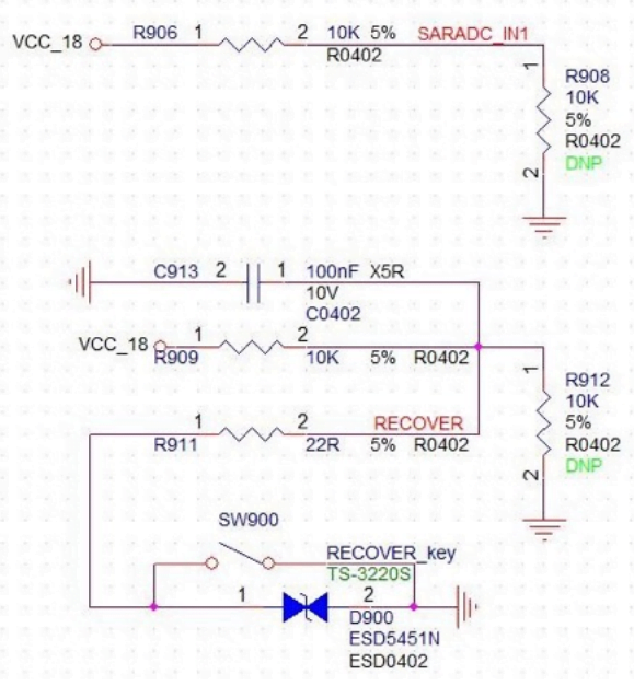
RK3328 uses SARADC_IN0 as the condition for entering RECOVER mode (without updating LOADER), as shown in the following figure. With firmware present, when SW900 is pressed at power on, SARADC_IN0 is kept at 0V, and RK3328 enters Rockusb programming mode. When the PC recognizes the USB device, release the button to restore ADC_IN0 to a high level (3.3V) and proceed with firmware programming.
For the convenience of online software debugging, RK3328 has a dedicated UART interface (UART2) for debugging purposes. In actual product applications, it is not recommended to use this interface for other functions. The interface should be designed as shown in Figure 3-46 to reserve a debugging interface for easy product debugging.
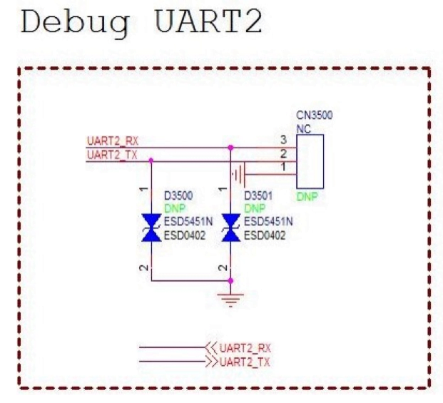
If an RS232 Voltage level conversion chip is used, attention should be paid to the TXD and RXD directions.
PCB layout recommendations: If the Debug function is frequently used (such as in development boards or SDKs), it is recommended to add ESD devices to the interface to provide protection for the chip. When laying out the mainboard, it should be convenient to solder the DEBUG line.
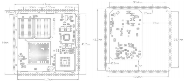
7. Product Dimensions of DSOM-010R RK3328 SOM
| Item | Parameter |
|---|---|
| Exterior | Stamp Hole |
| Core Board Size | 44mm X 44mm X 3.5mm |
| Pin Spacing | 1.2 mm |
| Pin Pad Size | 1.6mm X 0.65mm |
| Number of Pins | 132 Pins |
| Number of Layers | 8 floors |
| Warpage | less than 0.5 % |
8. The methods of Coreboard Thermal Control
There is a generic thermal system driver framework in the Linux kernel that defines a number of temperature control strategies. The following three strategies are currently in common use:
- Power_allocator: Introduces proportional-integral-derivative (PID) control, dynamically allocates power to each module based on the current temperature converts power to Frequency to achieve Frequency limiting based on temperature.
- Step_wise: Limits the Frequenof in steps based on the current temperature.
- User space: Does not limit Frequency.
The RK3328 chip has a T-sensor that detects the chip’s internal temperature and uses the Power_allocator strategy by default. The operating states are as follows:
- If the temperature exceeds the set temperature value:
■ If the temperature trend is rising, the Frequency is gradually reduced.
■ If the temperature trend is falling, the Frequency is gradually increased. - When the temperature falls to the set temperature value:
■ If the temperature trend is increasing, the Frequency remains unchanged.
■ If the temperature trend is falling, the Frequency is gradually increased. - Suppose the Frequency reaches its maximum and the temperature is still below the set value. In that case, the CPU frequency is no longer under thermal control, and the CPU frequency becomes system load frequency modulation.
- If the chip is still overheating after the Frequency has been reduced (e.g., due to poor heat dissipation) and the temperature exceeds 95 degrees, the software will trigger a restart. If the restart fails due to deadlock or other reasons and the chip exceeds 105 degrees, the otp_out inside the chip will trigger an immediate shutdown by the PMIC.
Note: The temperature trend is determined by comparing the previous and current temperatures. If the device temperature is below the threshold, the temperature is sampled every l seconds; if the device temperature exceeds the threshold, the temperature is sampled every 20ms, and the Frequency is limited.
The RK3328 SDK provides separate thermal control strategies for the CPU and GPU. Please refer to the (Rockchip_Developer_Guide_Thermal) document for specific configurations.
9. Production Guide of DSOM-010R RK3328 SOM
Select modules that can be SMT or in-line packaged according to the customer’s PCB design scheme. If the board is designed for SMT packaging, use SMT-packaged modules. If the board is designed for in-line assembly, use in-line assembly. Modules must be soldered within 24 hours of unpacking. If not, place them in a dry cabinet with a relative humidity of no more than 10% or re-pack them in a vacuum and record the exposure time (total exposure time must not exceed 168 hours).
Instruments or equipment required for SMT assembly:
- SMT Mounter
- SPI
- Reflow soldering
- Oven temperature tester
- AOI
Instruments or equipment required for baking:
- Cabinet ovens
- Antistatic high-temperature trays
- Antistatic and high-temperature gloves
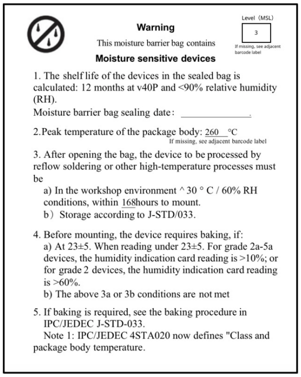
Moisture-proof bags must be stored at a temperature <40°C and humidity <90% RH. Dry-packed products have a shelf life of 12 months from the date of sealing of the package—sealed packaging with a humidity indicator card.
The vacuum bag is found to be broken before unpacking.
After unpacking, the bag is found to be without a humidity indicator card.
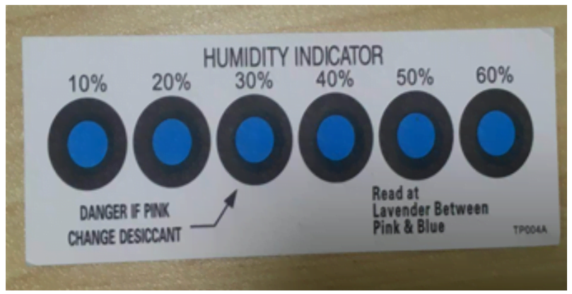
The humidity indicator card reads 10% or more after unpacking, and the color ring turns pink.
Total exposure time after unpacking exceeds 168 hours.
More than 12 months from the date of the first sealed packaging.
Baking parameters are as follows:
Baking temperature: 60°C for reel packs, humidity less than or equal to 5% RH;125°C for tray packs, humidity less than or equal to 5% RH (high-temperature-resistant trays, not blister packs for tow trays).
Baking time: 48 hours for reel packaging; 12 hours for pallet packaging.
Alarm temperature setting: 65°C for reel packs; 135°C for pallet packs.
After cooling to below 36°C under natural conditions, production can be carried out.
If the exposure time after baking is greater than 168 hours and not used up, bake again.
If the exposure time is more than 168 hours without baking, it is not recommended to use the reflow soldering process to solder this batch of modules. The modules are class 3 moisture-sensitive devices and may become damp when the exposure time is exceeded.
This may lead to device failure or poor soldering when high-temperature soldering is carried out.
Please protect the module from electrostatic discharge (ESD) during the entire production process.
To ensure product qualification rates, it is recommended to use SPI and AOI test equipment to monitor solder paste printing and placement quality.
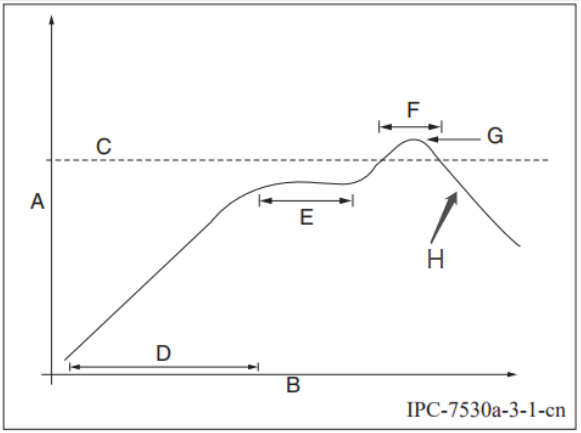
Description for graphs of curves.
A: Temperature axis
B: Time axis
C: Alloy liquid phase line temperature: 217-220°C
D: Slope of temperature rise: 1-3°C/s
E: Constant temperature time: 60-120s, constant temperature: 150-200°C
F: Time above liquid phase line: 50-70s
G: Peak temperature: 235-245°C
H: the slope of temperature reduction: 1-4°C/s
Note: above-recommended curves are based on SAC305 alloy solder paste as an example. Please set the recommended oven temperature curve for other alloy solder pastes according to the solder paste specification.
| Model | RAM | eMMC |
|---|---|---|
| DSOM-010R-L | 2GB | 8GB |
| DSOM-010R-N | 2GB | 32GB |
| DSOM-010R-M | 2GB | 16GB |
| DSOM-010R-K | 1GB | 8GB |
Documentations
DusunIoT offers full set of development resources including QUICK START, SDK, Firmware packaging, module firmware, Tools, vairous third party software,etc.