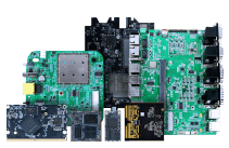
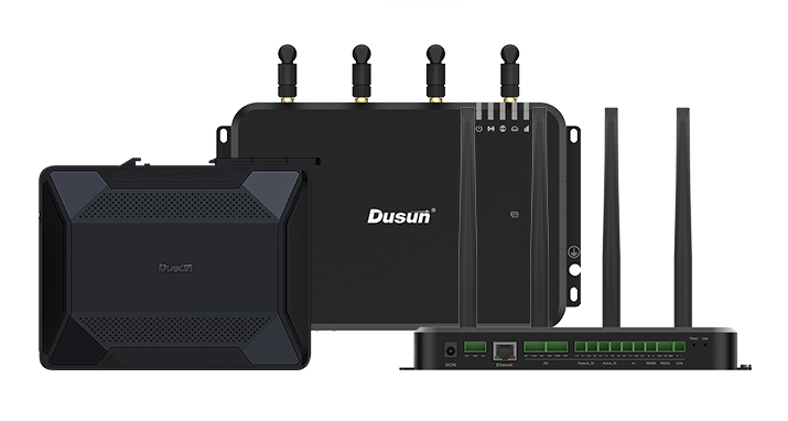
1. DSOM-020 PX30 SOM Purpose & Description
The DSOM-020R PX30 Stamp Hole System on Module adopts PX30 industrial 64-bit lowpower processor with quad-core 64-bit Cortex-A35, frequency up to 1.3 GHz, supports multiple operating systems, with powerful hardware decoding capability and a rich interface. such as I2C, UART, SPI, SPIO 3.0, USB2.0, PWN, RMII, I2S(supports 8-way digital microphone array input) and others interfaces.
The DSOM-020R PX30K System on Module is suitable for industrial control, power, communication, medical, media, security, vehicle, finance, consumer electronics, handheld devices, game consoles, display control, teaching instruments, and many other fields. It can be widely used in POS systems, game machines, teaching experiment platforms, multimedia terminals, PDAs, food ordering machines, advertising machines, and other fields.
The DSOM-020R System on Module offers a wide range of development documents and software resources that are both free and open-source. This convenience enables developers to enhance their development efficiency and shorten the development cycle.
- Featuring a compact form factor and sufficient GPIO interfaces
- Support for sleep/wake-up function
- Using RK809 PMU for Power Management Power ensures stable and reliable operation while keeping costs low enough
- Size 45mm*45mm
- eMMC up to 32GB
- RAM up to 2GB
- Support power sleep and wake-up
- Supports Buildroot, Linux + MiniGUI/QT, ROS
- Supports 100M wired Ethernet
- Leads out 144 PIN pins, including all CPU pins
- RoHS certified
- Stable and reliable product tested for high and low temperature, repeated reboot, Android stability, and AnTuTu benchmark
- l Work continuously for 7 days and 7 nights without crashing (or failing).
- AIOT equipment
- Vehicle control
- Game equipment
- Commercial display equipment
- Medical equipment
- Vending machines
- Industrial computers
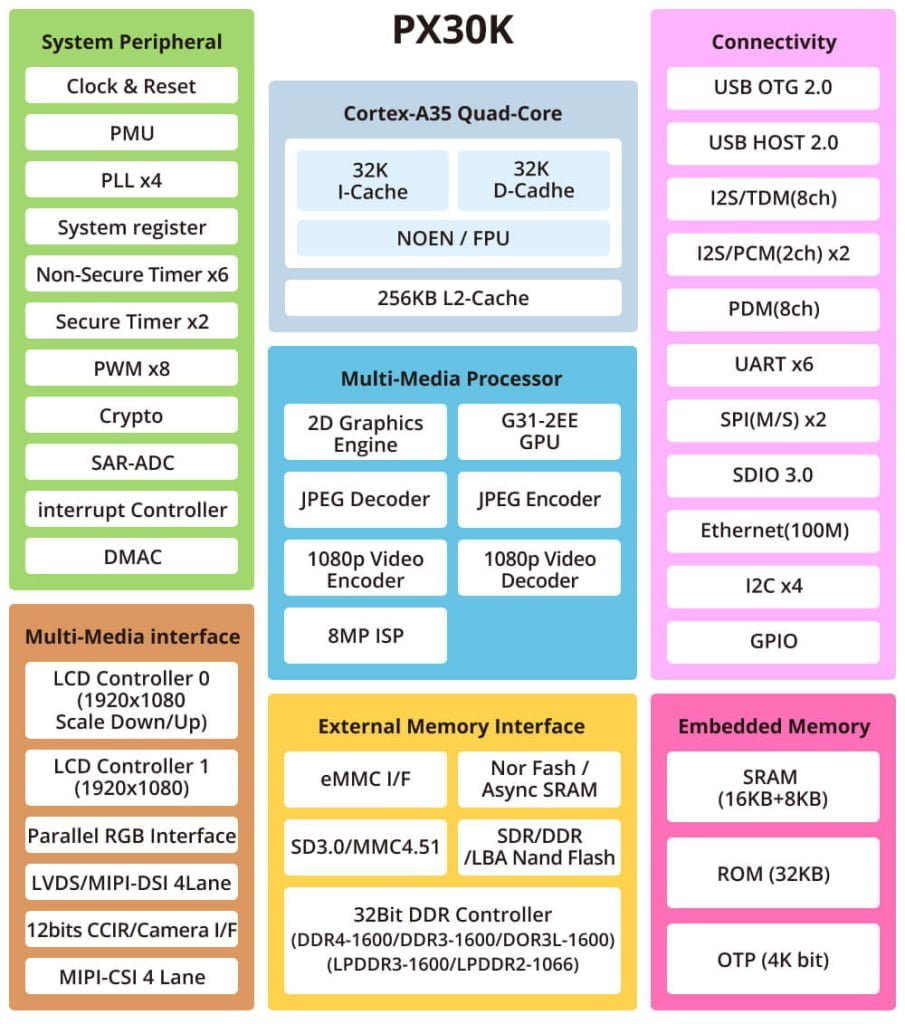
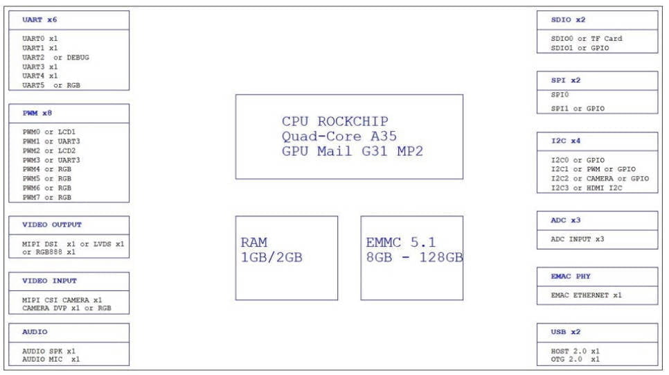
2. System Block Diagram of DSOM-020 PX30 SOM
3. Basic Parameters and Interfaces of DSOM-020 PX30 SOM
| Item | Parameter |
|---|---|
| CPU | Quad-core 64-bit Cortex-A35, frequency up to 1.3 GHz |
| GPU | Embedded ARM G31-2EE GPU makes the PX30K fully compatible with OpenGL ES 1.1/2.0/3.2, DirectX 11 FL9_3, OpenCL 2.0, and Vulkan 1.0. Built-in embedded high-performance 2D acceleration hardware |
| RAM | LPDDR3 2GB (1GB optional) |
| Storage | eMMC 32 GB (8GB / 16GB / 32GB /64GB / 128GB eMMC optional) |
| Power Management | RK809-1 Dynamic adjustment of the output voltage of each DC-DC converter |
| Operating Voltage | Typical voltage 5V/1.5A |
| RTC Input Voltage | Typical voltage 5V/30 uA |
| OS | Android / Debian |
| Temperature | Operating Temperature: -20 °C ~85 °C |
| Storage Temperature: -40 °C ~85 °C | |
| Humidity | 10~95% (Non-condensing) |
| Barometric Pressure | 76Kpa ~ 106Kpa |
| Size | 45mm x 45mm x 2.6mm |
| Item | Parameter |
|---|---|
| Ethernet | 1-channel 10M/100MHz Ethernet interface requires an external PHY chip |
| LCD | Support MIPI, LVDS, RGB Interface |
| Touch | Capacitive touch can be expanded with USB or serial port resistive touch |
| Audio | AC97 / IIS, Support recording and playback of audio |
| TF Card | 1 x SDIO Output Channel |
| I2S | 1 x 8-Channel I2S interface |
| SDIO | 1 x SDIO |
| eMMC | Onboard eMMC interface, the pins are not additionally led out |
| USB 2.0 | 2-channel USB 2.0 interface, one of which is a USB OTG interface |
| UART | 6 x Serial Port, except for UART2, the other four channels support serial flow control |
| PWM | 8 x PWM Output |
| I2C | 4 x I2C |
| SPI | 2 x SPI |
| ADC | 3 x ADC |
| Camera | 1 x MIPI CSI camera input interface or parallel camera input interface. |
| Upgrade | Support local upgrade via USB interface. |
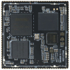
4. Pin Definition of DSOM-020 PX30 SOM
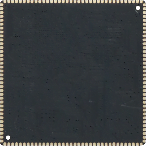
| Pin | Pin Definition | Pad Type | I/O Def | I/O Level (High/Low) Unit: mA |
I/O Driver (Unit: V) |
I/O Voltage (Unit: V) |
Functions |
|---|---|---|---|---|---|---|---|
| 1 | GPIO0_A5 | I/O | I | up | 2 | 3.0 | GPIO0_A5 |
| 2 | GPIO0_C2/I2C1_S C L/UART3_CTS |
I/O | I | down | 2 | 3.0 | GPIO or I2C pins or UART 3 flow control pin |
| 3 | GPIO0_C2/I2C1_S C L/UART3_CTS |
I/O | I | down | 2 | 3.0 | GPIO or I2C pins or UART 3 flow control pin |
| 4 | GPIO0_B4/UART0 _ CTS |
I/O | I | up | 2 | 3.0 | GPIO or UART 0 flow control pin |
| 5 | GPIO0_C0/PWM1 / UART3_TXD |
I/O | I/O | down | 2 | 3.0 | GPIO or UART 3 TXD or PWM pin |
| 6 | VCC3V3_LCD | P | N/A | N/A | 3.3V/2.5A power output | ||
| 7 | LVDS_TX0N/MIPI _T X_D0N/LCDC_D1 1_ M1 |
A | N/A | 3.3 | LCD Driver Interface | ||
| ... | ... | ... | ... | ... | ... | ... | ... |
NOTE:
I/O types: I = digital-input, O = digital-output, I/O = digital input/output (bidirectional)
A=Analog IO
Def default IO direction for digital IO
All GPIO pins support interrupts. P = power supply
VCC3V3_SYS, VCC3V0_PMU It is best not to supply power to these power outputs. They can be used as pull-up power supplies
5. Electrical Parameters of DSOM-020 PX30 SOM
| Parameter | Description | Min | Typ | Max | Unit |
|---|---|---|---|---|---|
| VCC5V0_SYS(_1/_2/_3) | VCC5V0_SYS Input voltage | -0.3 | 6.5 | V | |
| VCC_IO_RTC | RTC Input Voltage | -0.3 | 6.5 | V | |
| Ta | Operating temperature range | -20 | 85 | ℃ | |
| Ts | Store temperature range | -40 | 85 | ℃ |
Note:
Exposure to conditions beyond the absolute maximum ratings may cause permanent damage and affect the reliability and safety of the device and its systems.
The functional operations cannot be guaranteed beyond specified values in the recommended conditions.
| Parameter | Description | Min | Typ | Max | Unit |
|---|---|---|---|---|---|
| VCC5V0_SYS | VCC5V0_SYS Input Voltage | 4.75 | 5 | 5.5 | V |
| VCC_RTC | RTC Input Voltage | 4.75 | 5 | 5.5 | V |
| VCC5V0_SYS Supply Current | VCC5V0_SYS Input Current | 1 | A | ||
| VCC_RTC Supply Current | 30 | uA | |||
| Ta | Operating temperature | -20 | 25 | 85 | ℃ |
| Ts | Store temperature range | -40 | 25 | 85 | ℃ |
6. Hardware Design Guidelines of DSOM-020 PX30 SOM
The PX30K chip has two SPI controllers that can be used to connect SPI devices.
The recommended pull-up/pull-down and matching design for the SPI interface is shown in the table below
| Signal | Internal pull up/down |
Connection method | Description |
|---|---|---|---|
| SPI0_MOSI | Pull-down | Direct Connection | SPI data transmission |
| SPI0_MIS0 | Pull-up | Direct Connection | SPI data reception |
| SPI0_CLK | Pull-up | Series with 22ohm resistor | SPI clock transmission |
| SPI0_CSN | Pull-up | Direct Connection | SPI Slave Select Signal |
The PX30K chip provides an SDMMC interface controller that supports SD v3.0 and MMCv4.51 protocols. The recommended pull-up/pull-down and matching design for the SDMMC interface are shown in the table below
| Signal | Internal pull up/down |
Connection method (SDRHigh-Speedpeed Mode ) |
Description |
|---|---|---|---|
| SDMMC1_DQ[3:0] | Pull-up | Series with 22ohm resistor When the trace is short, it can be deleted |
SD data transmission / reception |
| SDMMC1_CLK | Pull-down | Series with 22ohm resistor | SD clock transmission |
| SDMMC1_CMD | Pull-up | Series with 22ohm resistor When the trace is short, it can be deleted |
SD command transmission/reception |
The PX30K chip has two sets of USB 2.0 interfaces, one supporting OTG mode and the other acting as a host. Please note the following when designing:
- USB interfaces are used as the default system firmware burning ort, and must
be reserved when designing. - USB_ID has a 200K internal pull-up resistor, which is pulled up to
- USB_AVDD_1V8, so OTG is set to Device mode by default.
- USB_DET (USB_VBUS) is used for USB insertion detection, and when it detects a high level, it means that USB has been inserted.
- To suppress electromagnetic radiation, it is recommended to reserve a common mode choke on the signal line. During debugging, use a resistor or common mode choke as appropriate.
| Signal | Connection Method | Description |
|---|---|---|
| USB_OTG_DP/DM | Direct Connection | USB OTG input/output |
| USB_ID | Direct Connection( Internal pull up) | USB OTG ID recognition, used for Micro-B interface |
| USB_DET | USB OTG insertion detection |
USB2.0 signal design rules:
- The intra-pair skew of differential pairs is less than 2ps;
- The length of differential pairs is less than 3 inches;
- The number of vias for differential pairs to change layers is less than 3;
- The impedance of differential pairs is controlled within 90ohm+/-10%;
- The spacing between differential pairs and other signals follows the 3W principle.
PX30K provides three standard I2S interfaces, all supporting master and slave modes with a maximum sampling rate of 192kHz and a bit rate ranging from 16 bits to 32 bits.
● I2S0
The I2S0 interface of the PX30K provides the independent 8-channel output and 8- channel input. To meet the needs of asynchronous sampling rates for playback and recording, two sets of bit clocks and frame clocks (SCLKTX/ LRCKTX, SCLKRX/ LRCKRX) are also provided. It should be noted that for the case where only one set of bit/frame clocks is referenced for SDOx and SDIx, SCLKTX/LRCKTX is preferred as their standard clock.
| Signal | Internal pull up/down |
Connection method | Description |
|---|---|---|---|
| I2S0_8CH_MCLK | Pull-down | Series with 22ohm resistor | I2S0 System clock output |
| I2S0_8CH_SCLKTX | Pull-down | Series with 22ohm resistor | I2S0 Bit clock (TX, Associated with SDOx) |
| I2S0_8CH_LRCKTX | Pull-down | Series with 22ohm resistor | I2S0 Frame clock output for channel selection clock ( TX, Associated with SDOx) |
| I2S0_8CH_SDO0 | Pull-down | Series with 100ohm resistor | I2S0 Data output channel 0 |
| I2S0_8CH_SDO1 | Pull-down | Series with 22ohm resistor | I2S0 Data output channel 1 |
| I2S0_8CH_SDO2 | Pull-down | Series with 22ohm resistor | I2S0 Data output channel 2 |
| I2S0_8CH_SDO3 | Pull-down | Series with 22ohm resistor | I2S0 Data output channel 3 |
| I2S0_8CH_SCLKRX | Pull-down | Series with 100ohm resistor | I2S0 Bit clock (RX, Associated with SDIx) |
| I2S0_8CH_LRCKRX | Pull-down | Series with 22ohm resistor | I2S0 Frame clock output for channel selection clock ( RX, Associated with SDIx) |
| I2S0_8CH_SDI0 | Pull-down | Series with 22ohm resistor | I2S0 Data output channel 0 |
| I2S0_8CH_SDI1 | Pull-down | Series with 22ohm resistor | I2S0 Data output channel 1 |
| I2S0_8CH_SDI2 | Pull-down | Series with 100ohm resistor | I2S0 Data output channel 2 |
| I2S0_8CH_SDI3 | Pull-down | Series with 22ohm resistor | I2S0 Data output channel 3 |
● I2S1
I2S1 supports 2-channel input and 2-channel output. The pull-up and matching design recommendations for the I2S1 interface are shown in the following table.
| Signal | Internal pull up/down |
Connection method | Description |
|---|---|---|---|
| I2S1_MCLK | Pull down | Series with 22ohm resistor | I2S1 System clock output |
| I2S1_SCLK | Pull down | Series with 22ohm resistor | I2S1 Bit clock output |
| I2S1_LRCK_TXRX | Pull down | Series with 22ohm resistor | I2S1 Frame clock output for channel selection clock |
| I2S1_SDO | Pull down | Series with 22ohm resistor | I2S1 Data output channel |
| I2S1_SDI | Pull down | Series with 22ohm resistor | I2S1 Data input channel |
● I2S2
I2S2 supports 2-channel output and 2-channel input and is used by default to connect to the PCM interface of the BT module, serving as the communication port for the Bluetooth call function under the HFP protocol.
The recommended pull-up and matching design for the I2S2 interface is shown in the following table.
| Signal | Internal pull up/down |
Connection method | Description |
|---|---|---|---|
| I2S2_2CH_MCLK | Pull down | Series with 22ohm resistor | I2S0_2CH system clock output No PCM function multiplexing can be used as a normal GPIO |
| I2S2_2CH_SCLK PCM_CLK |
Pull down | Series with 22ohm resistor | I2S0_2CH bit clock output PCM clock |
| I2S2_2CH_LRCK PCM_SYNC |
Pull down | Series with 22ohm resistor | I2S0_2CH Frame clock output for channel selection clock PCM Data frame synchronisation |
| I2S2_2CH_SDO PCM_OUT |
Pull down | Series with 22ohm resistor | 2S0_2CH Data output channel PCM data output |
| I2S2_2CH_SDI PCM_IN |
Pull down | Series with 22ohm resistor | 2S0_2CH Data input channel PCM data Input |
PX30K provides one set of PDM digital audio interfaces, supporting up to 8 channels of PDM format audio input with a maximum sampling rate of 192kHz and bit rates ranging from 16bits to 32bits.
To cooperate with RK809-1 to achieve audio input, the IO multiplexing here is relatively flexible, and care should be taken to avoid repeated use of the same signal in different multiplexing positions. When using PDM MIC as voice input, to simplify the software processing of audio recording data, it is recommended to use the PDM interface consistently for both recording and input. This way, for the common application scenarios involving 2-6 PDM MIC recording channels and 1-2 channels of input, only one complete 4-8 channel recording audio is needed, and no extra splicing processing is required in the software.
If you need to connect 8-channel PDM MIC input, you can only use the I2S interface as the capture channel for input. Software needs to perform additional audio splicing processing to meet the requirements of the algorithm for data synchronization.
● Codec
RK809-1 comes with a codec and is connected to PX30K via the I2S interface. The HPSNS output of the codec serves as an internal offset reference and needs to be connected to GND. The routing should be connected to GND at the headphone jack to reduce the potential difference between the codec and the headphone GND. If the codec’s GND is on the same complete GND plane as the headphone GND and the device layout is close, it can be directly connected to the GND plane.
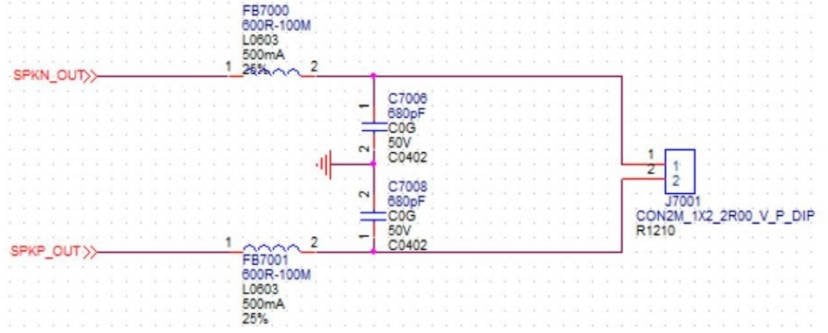
The codec has a built-in mono non-filtered speaker driver circuit that can provide 1.3W@8ohm of driving power, which meets the application requirements of small power monaural scenarios and can save additional external amplifier costs. When using this built-in amplifier, the recommended audio input circuit is as follows: after voltage division and filtering, the differential feedback signal is output to the audio ADC interface of RK809-1 and then passed back to PX30K through the PDM/I2S interface after A/D conversion by RK809-1.
The default setting for RK809-1 here is PDM interface communication with PX30K, which is based on the consideration of using PDM microphones, as described in the PDM interface section.
● MIC
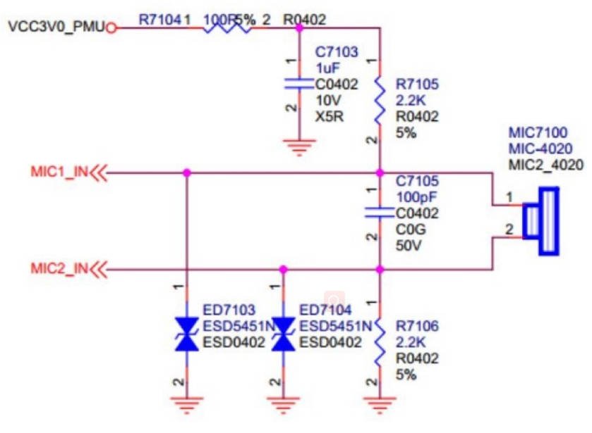
The MIC circuit is shown in the following diagram. Please select appropriate voltage divider resistors R7105 and R7106 according to the specifications of the electret microphone. If an analog interface MEMS MIC is used, please refer to the specifically recommended design circuit. If a digital interface MEMS MIC is used, it can be directly connected to the I2S0 of PX30K.
Video Interface The PX30K chip has a built-in video controller that supports three video output modes: RGB, LVDS, and MIPI DSI.
LVDS/MIPI Mode
LVDS/MIPI uses the same controller, and some pins are shared with RGB. When using LVDS/MIPI output, the software needs to configure the corresponding output mode.
LVDS/MIPI signal design rules:
- Differential pair offset within 2ps.
- The differential pair group offset between Clk and Data is less than 3.5ps.
- The differential pair length is less than 3.6 inches.
- The number of through-holes for differential pairs to change layers is less than 3.
- Differential pair impedance is controlled within 100ohm+/-10%.
- The distance between differential pairs and other signals follows the 3W
principle.
RGB Mode
PX30K supports 24-bit RGB output. When using RGB output, the software needs to configure the corresponding output mode.
When using an RGB888 24-bit screen, the corresponding signal relationship is as follows:
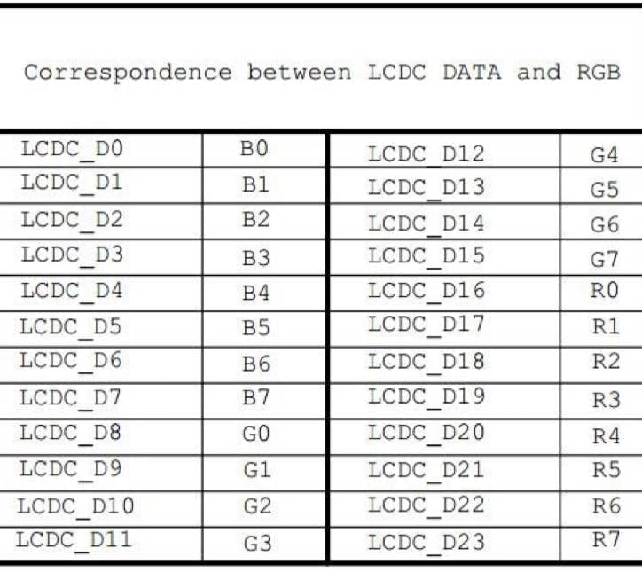
When using an 18-bit RGB666 screen, only the LCDC_D0-D17 data signals need to be connected, and the corresponding signal relationship is as follows:
MIPI CSI
PX30K has a MIPI-CSI input with a built-in ISP processor.
MIPI signal design rules:
- Differential pair offset within 2ps.
- The differential pair group offset between Clk and Data is less than 3.5ps.
- The differential pair length is less than 3.6 inches.
- The number of through-holes for differential pairs to change layers is less than 3.
- Differential pair impedance is controlled within 100ohm+/-10%.
- The distance between differential pairs and other signals follows the 3W principle.
CIF CAMERA
The power supply domain for the CIF interface is 3.0V. In the actual product design, the corresponding power supply should be selected based on the actual IO power supply requirements of the camera (1.8V or 2.8V), and the I2C pull-up voltage level must be consistent with it. Otherwise, it will cause the camera to malfunction or not work. The CIF interface pins are multiplexed with the RMII pins.
RMII Circuit
The RMII and CIF interfaces can be multiplexed and configured to support 100Mbps Ethernet PHY, enabling the implementation of 100Mbps network functionality. Please refer to the PHY manufacturer’s design documentation for details on designing a 100Mbps network. The clock signal required by the PHY can be generated by an external crystal or provided by the chip’s MAC_CLK signal.
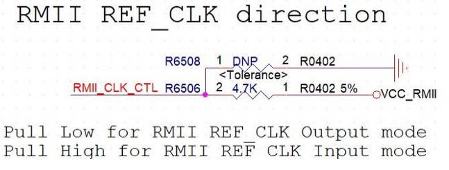
The PX30K chip uses the SARADC’s ADC_IN2 as the key input sampling port and also for RECOVER mode (which does not require updating LOADER). With the firmware already burned into the system, pulling ADKEY_IN low during system startup will keep ADC_IN2 at a 0V level, allowing PX30K to enter the Rockusb firmware writing mode. When the PC recognizes the USB device, release the button to restore ADC_IN2 to a high level (1.8V), and then the firmware writing can be carried out.
On PX30K, the SARADC sampling range is 0-1.8V, and the sampling accuracy is 10 bits. The parallel-type key array can adjust the input key value by adding or reducing keys and adjusting the voltage divider ratio to achieve multi-key input to meet customer product requirements. In design, it is recommended that any two key values must be greater than +/- 35, which means that the center voltage difference must be greater than 123 mV.The pull-up and matching design recommended for the SDIO1 interface is shown in the following table.
PX30K supports WIFI/BT modules with SDIO 3.0 interface. When using WIFI/BT modules with SDIO1 and UART interfaces, it is important to ensure that the power supply of PX30K’s SDIO1 and UART1 controllers is consistent with the IO level of the module.
● SDI0
The recommended pull-up/down and matching design for the SDMMC0 interface are as follows:
| Signal I | Internal pull up/down |
Connection method | Description |
|---|---|---|---|
| SDI0_DQn[3:0] | Pull Up | Series with 22ohm resistor The routing can be removed temporarily for shorts |
SDI0 data transmission and reception |
| SDI0_CLK | Pull Down | Series with 22ohm resistor | SDI0 clock signal transmission |
| SDI0_CMD | Pull Down | Series with 22ohm resistor The routing can be removed temporarily for shorts |
SDI0 data transmission and reception |
● UART
The recommended pull-up/down and matching design for the SDMMC1 interface are as follows:
| Signal | Internal pull up/down |
Connection method | Description |
|---|---|---|---|
| UART1_RX | Pull up | Direct Connection | UART1 Data input |
| UART1_TX | Pull up | Direct Connection | UART1 Data output |
| UART1_CTSn | Pull up | Direct Connection | UART1 allows signal transmission |
| UART1_RTSn | Pull up | Direct Connection | UART1 requests signal transmission |
7. Product Patameter of DSOM-020 PX30 SOM
| Item | Parameter |
|---|---|
| Exterior | Stamp Hole |
| Core Board Size | 45mm x 45mm x 2.6mm |
| Pin Spacing | 1.2mm |
| Pin Pad Size | 2.0mm x 0.7mm |
| Number of Pins | 144 Pins |
| Warpage | less than 0.5 % |
8. The methods of Coreboard Thermal Control
There is a generic thermal system driver framework in the Linux kernel that defines a number of temperature control strategies. The following three strategies are currently in common use:
- Power_allocator: Introduces proportional-integral-derivative (PID) control,
dynamically allocates power to each module based on the current temperature,
and converts power to frequency to achieve frequency limiting based on
temperature. - Stepwise: Limits the frequency of steps based on the current temperature.
- User space: Does not limit frequency.
The RK3568 chip has a T-sensor that detects the chip’s internal temperature and uses the Power_allocator strategy by default. The operating states are as follows:
- If the temperature exceeds the set temperature value:
– If the temperature trend is rising, the frequency is gradually reduced.
– If the temperature trend is falling, the frequency is gradually increased. - When the temperature falls to the set temperature value:
– If the temperature trend is increasing, the frequency remains unchanged.
– If the temperature trend is falling, the frequency is gradually increased. - If the frequency reaches its maximum and the temperature is still below the set value, the CPU frequency is no longer under thermal control, and the CPU frequency becomes system load frequency modulation.
- If the chip is still overheating after the frequency has been reduced (e.g., due to poor heat dissipation) and the temperature exceeds 95 degrees, the software will trigger a restart. If the restart fails due to deadlock or other reasons and the chip exceeds 105 degrees, the otp_out inside the chip will trigger a direct shutdown by the PMIC.
Note: The temperature trend is determined by comparing the previous and current temperatures. If the device temperature is below the threshold, the temperature is sampled every l seconds; if the device temperature exceeds the threshold, the temperature is sampled every 20ms, and the frequency is limited.
The RK3568 SDK provides separate thermal control strategies for the CPU and GPU. Please refer to the (Rockchip_Developer_Guide_Thermal) document for specific configurations.
9. Production Guide of DSOM-020 PX30 SOM
Select modules that can be SMT or in-line packaged according to the customer’s PCB design scheme. If the board is designed for SMT packaging, use SMT-packaged modules. If the board is designed for in-line assembly, use in-line assembly.
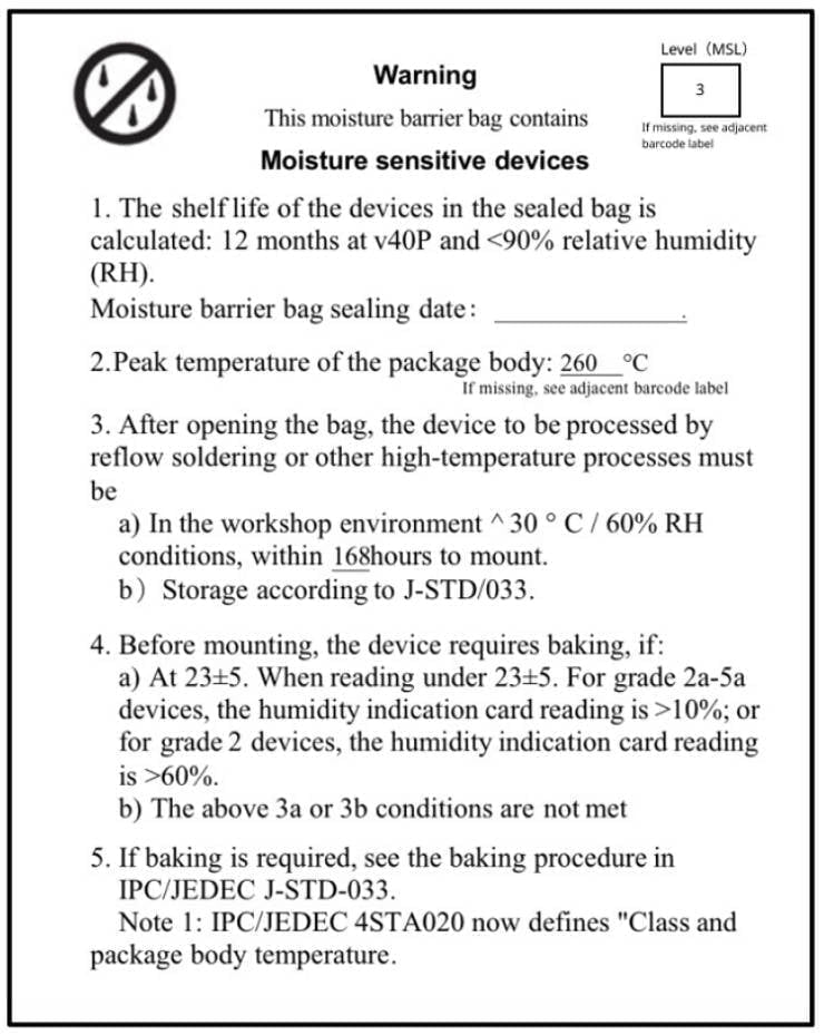
Modules must be soldered within 24 hours of unpacking. If not, place them in a dry cabinet with a relative humidity of no more than 10% or re-pack them in a vacuum and record the exposure time (total exposure time must not exceed 168 hours).
Instruments or equipment required for SMT assembly:
- SMT Mounter
- SPI
- Reflow soldering
- Oven temperature tester
- AOI
Instruments or equipment required for baking:
- Cabinet ovens
- Antistatic high-temperature trays
- Antistatic and high-temperature gloves
Moisture-proof bags must be stored at a temperature <40°C and humidity <90% RH. Dry-packed products have a shelf life of 12 months from the date of sealing of the package. Sealed packaging with humidity indicator card.

The vacuum bag is found to be broken before unpacking.
After unpacking, the bag is found to be without a humidity indicator card. The humidity indicator card reads 10% or more after unpacking, and the color ring turns pink.
Total exposure time after unpacking exceeds 168 hours. More than 12 months from the date of the first sealed packaging.
Baking parameters are as follows:
Baking temperature: 60°C for reel packs, humidity less than or equal to 5% RH; 125°C for tray packs, humidity less than or equal to 5% RH (high-temperatureresistant trays, not blister packs for tow trays).
Baking time: 48 hours for reel packaging; 12 hours for pallet packaging.
Alarm temperature setting: 65°C for reel packs; 135°C for pallet packs.
After cooling to below 36°C under natural conditions, production can be carried out.
If the exposure time after baking is greater than 168 hours and not used up, bake again.
If the exposure time is more than 168 hours without baking, it is not recommended to use the reflow soldering process to solder this batch of modules. The modules are class 3 moisture-sensitive devices and may become damp when the exposure time is exceeded.
This may lead to device failure or poor soldering when hightemperature soldering is carried out.
Please protect the module from electrostatic discharge (ESD) during the entire production process.
To ensure product qualification rates, it is recommended to use SPI and AOI test equipment to monitor solder paste printing and placement quality.
Please follow the reflow profile for SMT placement with a peak temperature of 245°C. The reflow temperature profile is shown below using the SAC305 alloy solder paste as an example.
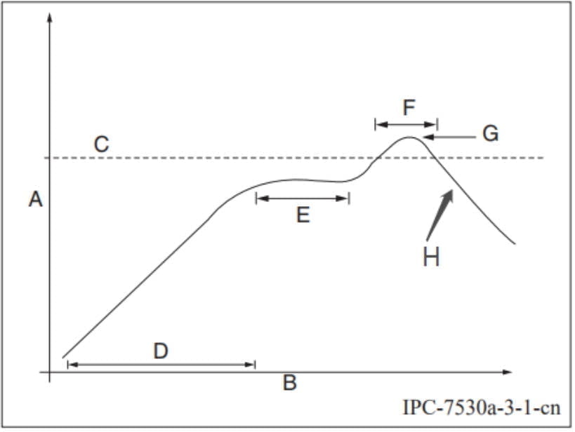
Description for graphs of curves.
A: Temperature axis
B: Time axis
C: Alloy liquid phase line temperature: 217-220°C
D: Slope of temperature rise: 1-3°C/s
E: Constant temperature time: 60-120s, constant temperature: 150-200°C
F: Time above liquid phase line: 50-70s
G: Peak temperature: 235-245°C
H: slope of temperature reduction: 1-4°C/s
Note: The above recommended curves are based on SAC305 alloy solder paste as an example. Please set the recommended oven temperature curve for other alloy solder pastes according to the solder paste specification.
| Model | RAM | eMMC |
|---|---|---|
| DSOM-020R-K | 1GB | 8GB |
| DSOM-020R-N | 2GB | 32GB |
| DSOM-020R-P | 2GB | 128GB |
Documentations
DusunIoT offers full set of development resources including QUICK START, SDK, Firmware packaging, module firmware, Tools, vairous third party software,etc.

