1. Product Introduction
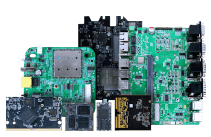
Based on Rockchip RK3588 Designed for Static mapping machine A high-performance Embedded motherboard products. DSK-070 has an 8-core CPU, 6TOPS independent NPU computing power, strong AI capabilities, and includes USB and MIPI rich peripheral interfaces to fully meet Access requirements for robot multi-sensor perception and control blocks, suitable for harsh outdoor environments. It supports flexible selection of operating systems, with Android system as standard, and can also independently run Android/Linux+RTOS fusion operating system. It is mainly used in mapping robot scenarios that require high performance and high computing power.
| Name | Describe |
|---|---|
| Product Model | DSGK-070 |
| CPU | RK3588 |
| RAM | 8GB |
| EMMC | 128GB |
| System | Android 12 |
| PCIE3.0 | 4Lan, 2280 external SSD, maximum capacity up to 2TB |
| Network port | 1 10/100/1000Mbps Ethernet interface |
| USB3.0 interface | 2 USB3.0 HOST interfaces, 1 USB3.0 OTG interface |
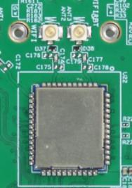
| Wi-Fi | Wi-Fi6, 802.11a/b/g/n/ac/ax 1200Mbps WLAN + BT v5.2, 2 ipex antenna sockets |
| Audio | Support, can connect an external 8 ohm/2W speaker |
| video | Support, 1 MIPI DSI interface, 4Lan |
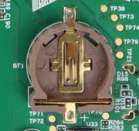
| RTC | Yes, with spare CR1220 battery holder for non-rechargeable batteries |
| Debug interface | Support, 1 UART interface on board |
| button | 1 power button |
| 1 hard reset button | |
| 1 RECOVERY button | |
| 1 MASKROM button | |
| Cooling Solution | Support radiator + fan |
| Sensor interface | Support external six-axis gyroscope sensor and magnetometer sensor |
| LED | Flash control interface |
| Bluetooth working status indicator light control interface | |
| Wifi working status indicator light control interface | |
| power supply | DC power supply voltage range 12V/2A and battery power supply voltage range 9V to 12V |
| Operating temperature | -10 to 70 degrees |
| Storage temperature | -20 to 80 degrees |
| PCBA Dimensions | 100*101.5mm |
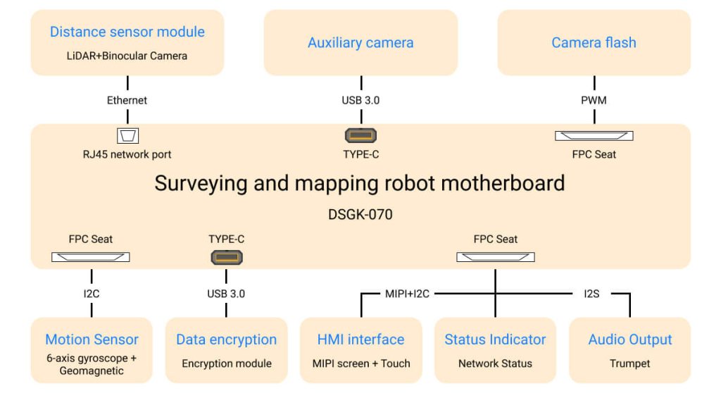
Dusun integrates relevant applications of the robotics industry on the basis of standard systems. custom made High reliability Operating system and industry SDK, With many years of experience in the development and design of robot embedded motherboards, we have completed the transplantation and testing of various hardware peripheral drivers that meet industry applications. The following is the software framework of the default Android system of DSGK-070.
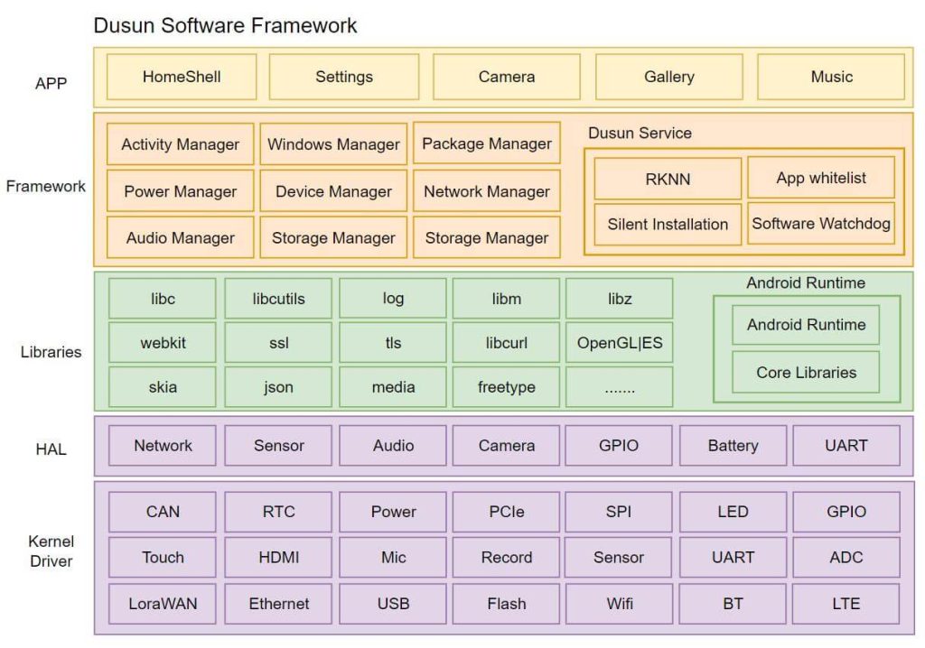
In addition, Dusun can Provide independent system support for various versions of Linux, such as Debian, Ubuntu, etc.It can also support the multi-core fusion system of AMP Android/Linux +ROTS, and has good performance in real-time control and complex algorithm support.
Dusun provides the robot industry SDK source code that matches the surveying and mapping robot motherboard, supporting customers to conduct micro-development to achieve rapid productization. Dusun Robot Industry The SDK has the following features:
1. Streamlined operating system: On the premise of meeting industry applications, the number of components is streamlined, the system resource utilization rate is high, thereby reducing hardware costs, and to a certain extent, the functional structure is optimized, the system architecture is reasonably laid out, and the system is more efficient and easy to maintain;
2. BSP with industry attributes: According to the types of peripheral devices used in the industry, driver transplantation and debugging are carried out and industry algorithms are adapted to meet the customer’s needs for selecting an overall hardware + algorithm solution. In addition, Dusun BSP driver will continue to iterate the access to peripheral devices of different brands and models.
3. Pre-installed tools and middleware: Pre-install NPU’s big data model tools (such as ONXX, etc.) and the middleware ROS/ROS2 of the robotics industry in advance, so that users can quickly transplant applications and tree models of other hardware platforms and achieve low-cost hardware platform switching.
| Peripherals | model | illustrate |
|---|---|---|
| fan | DB7505h05S | Support PWM speed control Support speed FG signal reading back |
| trumpet | -- | 8W speaker |
| MIPI Touch LCD | Hongguang HG050HD026T01 | Resolution 720x1280 Capacitive touch |
| USB Camera | -- | Universal UVC |
| External expansion USB flash drive | TinkPad/Patriot/Kingston mainstream models | Universal 3.0/2.0 USB flash drive |
| Core Algorithm | Matching peripheral hardware | model | illustrate |
|---|---|---|---|
| SLAM Algorithm |
LiDAR + Binocular Camera | SLAMTEC Aurora | |
| Magnetometer | AK09915c | ||
| Six-axis gyroscope | ICM-42688 | ||
| Face recognition algorithm | Structured light module | RMSL321 | RK NN Deep Algorithm |
| Intelligent voice algorithm | 6-microphone circular array | Can be customized according to structure | Sound pickup and noise reduction, keyword wake-up, voice wake-up |
| Monocular ranging algorithm | Structured light module | RMSL321 | Distance and angle information of visual obstructions |
Note: The above algorithms are not pre-installed in the factory firmware version. If necessary, please contact the corresponding technical window
Big data model tools are pre-installed in the product SDK: RKNN API, TensorFlow Lite; ONNX Runtime; ONNX Runtime, Android NNAPI
2. Installation Instructions
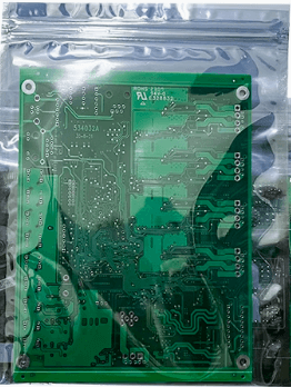
1.Shipping packaging bag: anti-static sealing bag (as shown below);
3.Product weight: 150g±5g;
4.The product is packed in boxes, 100 pieces per box, as shown in the following figure. (One piece of product is placed in a gap, and there are two layers of gaps in total, which can hold 100 pieces of products)
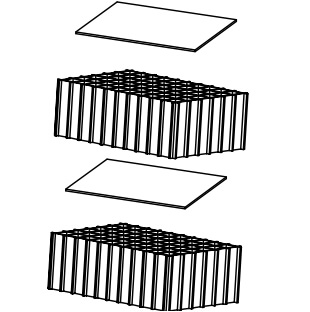

1、The product leaves the factory without accessories
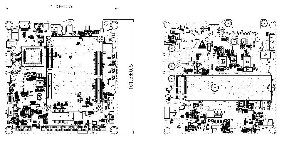
1、The product is fixed by 4 screws (the fixing hole positions are shown in the figure below). The screw hole diameter is 3.3±0.15mm. It is recommended to use M3mm cross pan head screws.
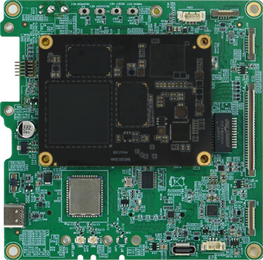
2、The product can be equipped with a core board and a core board radiator. The radiator size is recommended to be as follows:
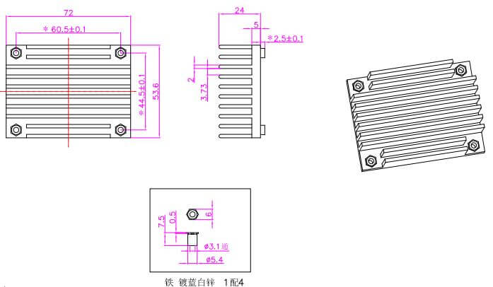
The radiator is fixed to the product with 4 screws. The recommended screw specifications are: M2X14mm, cross pan head screws.
3.It is recommended that both sides of the board be limited to ≥45mm (depending on the actual shell design requirements)
3. Hardware Instructions
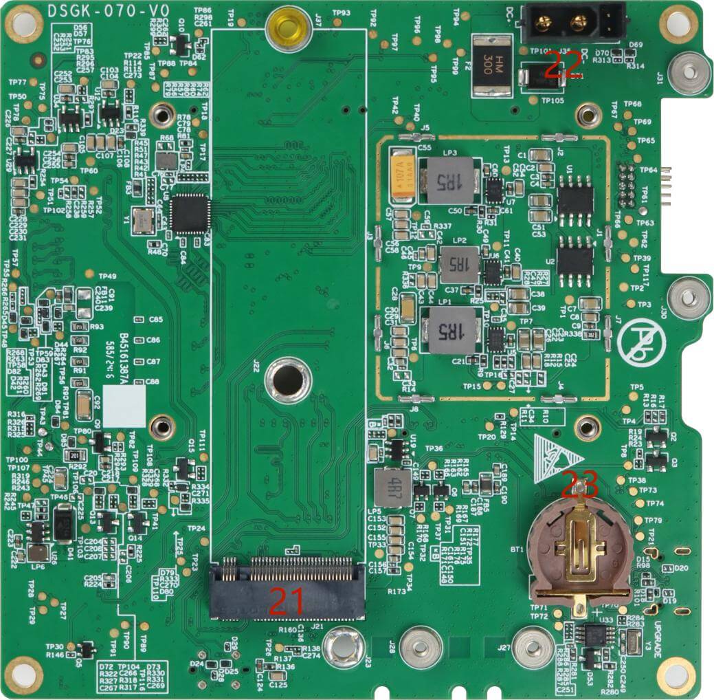
| Serial number | describe | Remark |
|---|---|---|
| 1 | Power button | Not external, for debugging |
| 2 | RECOVERY button | |
| 3 | Hard reset button | |
| 4 | MASKROM button | |
| 5 | Fan connector | Reserved core board cooling fan interface |
| 6 | USB3.0 HOST0 interface | External USB flash drive |
| 7 | Flash control interface | External flash light board |
| 8 | 60pin adapter | The 60-pin pins include: power supply input pin; 1 8 ohm/2W speaker interface; screen backlight driver; Wifi working status indicator light control interface; screen touchpad control interface; Ethernet interface; screen MIPI DSI interface and other control signals |
| 9 | USB3.0 HOST2 interface | Connecting a Camera |
| 10 | Debug interface | 1 UART interface, CMOS level, level 3.3V, 1.25mm pitch, 3Pin socket |
| 11 | USB3.0 OTG interface | Type C interface, external dongle |
| 12 | Wifi module | Wifi6 module, 802.11a/b/g/n/ac/ax 1200Mbps WLAN + BT v5.2, SDIO interface, 2 ipex antenna sockets |
| 13 | Wifi main antenna for Wifi | |
| 14 | Wifi secondary antenna and Bluetooth 2-in-1 antenna | |
| 15 | After the ipex sockets 13 and 14 are installed with antennas, a board will be used to press the connector of the ipex antenna, and 15 and 16 will fix the pressing board with screws. | The recommended fixing screw size is M2*4mm |
| 16 | ||
| 17 | Firmware burning interface | Software program for burning PCBA |
| 18 | Bluetooth working status control interface | |
| 19 | Sensor interface | External sensor board, which has six-axis accelerometer and magnetometer sensor |
| 20 | RK3588 core board | The core board is connected to the main board through four board-to-board connectors, and the four nut columns on the main board are used to fix the core board. The capacity of the core board RAM is 8GB, and the capacity of the EMMC is 128GB |
| twenty one | SSD interface | It uses an M.2 slot, PCIE3.0 4Lan, and can expand a 2280 solid-state hard drive with a maximum capacity of 2TB |
| twenty two | System backup battery interface | Used for external 12V lithium battery, the lithium battery itself has power measurement function |
| twenty three | RTC Backup Battery Holder | CR1220 battery holder, for non-rechargeable batteries |
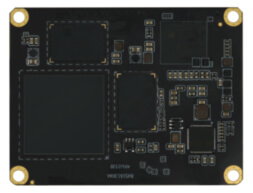
①The mainboard uses the Dusun RK3588 core board (DSOM-040R). The position of the core board on the PCBA is shown in the figure below:
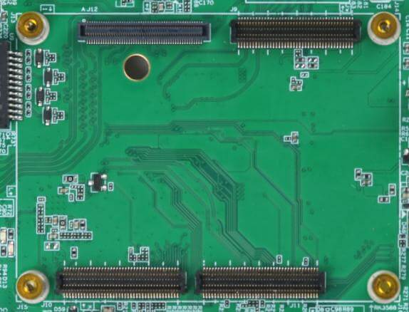
In the above figure, J13, J14, J15 and J16 are the four columns for fixing the core board. The size parameter is M2*3.0, and the corresponding fixing screw size can be M3*6.0mm.
②The actual picture of the core board is shown below:

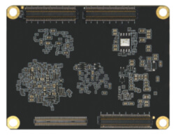
The core board used on this PCBA has a RAM capacity of 8GB and an EMMC capacity of 128GB.
①The pin sequence of the 60-pin interface J34 on the PCBA is shown in the figure below:
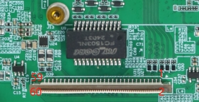
| Serial number | Pin Name | Pin Description | IO level | Remark |
|---|---|---|---|---|
| 1 | GND | Signal Ground | 0V | |
| 2 | MIPI_TX_D0N | MIPI DSI Signaling | Connect to display screen | |
| 3 | MIPI_TX_D0P | MIPI DSI Signaling | ||
| 4 | GND | Signal Ground | 0V | |
| 5 | MIPI_TX_D1N | MIPI DSI Signaling | Connect to display screen | |
| 6 | MIPI_TX_D1P | MIPI DSI Signaling | ||
| 7 | GND | Signal Ground | 0V | |
| 8 | MIPI_TX_CLKN | MIPI DSI Signaling | Connect to display screen | |
| 9 | MIPI_TX_CLKP | MIPI DSI Signaling | ||
| 10 | GND | Signal Ground | 0V | |
| 11 | MIPI_TX_D2N | MIPI DSI Signaling | Connect to display screen | |
| 12 | MIPI_TX_D2P | MIPI DSI Signaling | ||
| 13 | GND | Signal Ground | 0V | |
| 14 | MIPI_TX_D3N | MIPI DSI Signaling | Connect to display screen | |
| 15 | MIPI_TX_D3P | MIPI DSI Signaling | ||
| 16 | GND | Signal Ground | 0V | |
| 17 | TP_VCC3V3 | Touchpad I3.3V power supply | 3.3V | Touch panel power supply |
| 18 | TP_I2C_SCL | Touchpad I2C signal | 1.8V | Touch screen communication interface |
| 19 | TP_I2C_SDA | 1.8V | ||
| 20 | TP_nINT | Touchpad interrupt signal | 1.8V | Screen touch panel interrupt output pin |
| 21 | TP_nRST | Touchpad reset signal | 1.8V | Touch screen reset pin, low level is effective |
| 22 | MIPI_LCD_VCC3V3 | Display screen I3.3V power supply | 3.3V | Display screen power supply |
| 23 | MIPI_VCCIO_1V8 | Display VCCIO power supply | 1.8V | Power supply for the IO signal pins of the display |
| 24 | MIPI_LCD_nRST | Display reset signal | 1.8V | Display reset pin, low level is effective |
| 25 | GND | Signal Ground | 0V | |
| 26 | DD0- | 10M/100M/1000Mbps Ethernet network transformer primary side signal | This signal can be directly connected to the RJ45 socket | |
| 27 | DD0+ | |||
| 28 | DC0- | |||
| 29 | DC0+ | |||
| 30 | DB0- | |||
| 31 | DB0+ | |||
| 32 | DA0- | |||
| 33 | DA0+ | |||
| 34 | GND | Signal Ground | 0V | |
| 35 | SET_PWM | Flash light drive signal | 3.3V | To connect to the flash interface |
| 36 | EN_FLASH | 3.3V | ||
| 37 | SOM_IO_PWR_CHK_H | Power on successfully output pin | 3.3V | After the power-on is successful, this pin outputs a high level |
| 38 | EN_SOM_POWER | Mainboard power enable signal | 3.3V | High level is effective |
| 39 | IO_FPGA_PHONE_ON | Display wake-up signal | 3.3V | Rising edge is valid, default is low level. |
| 40 | SOM_IO_PWR_OFF_t | Soft shutdown signal | 3.3V | Rising edge valid , default low level |
| 41 | I2C7_SDA_M3 | Fuel meter I2C interface | 3.3V | This signal is connected to the battery's fuel gauge chip |
| 42 | I2C7_SCL_M3 | 3.3V | ||
| 43 | NC | Dangling | ||
| 44 | NC | |||
| 45 | NC | |||
| 46 | NC | |||
| 47 | NC | |||
| 48 | WIFI_LED_K | Wif working status indicator cathode | 5V | This signal is connected to an external LED light board |
| 49 | WIFI_LED_A | Wif working status indicator light anode | 5V | |
| 50 | GND | Signal Ground | 0V | |
| 51 | BK_LED_K | Display backlight driver cathode | ||
| 52 | BK_LED_A | Display backlight driver anode | ||
| 53 | GND | Signal Ground | 0V | |
| 54 | SPK_VOP | Speaker positive terminal | External 8 ohm/2W trumpet |
|
| 55 | SPK_VON | Negative pole of the speaker | ||
| 56 | GND | Signal Ground | 0V | |
| 57 | DC_IN | System power supply | Supply voltage 12+5%, 2A | External DC power input |
| 58 | DC_IN | |||
| 59 | DC_IN | |||
| 60 | DC_IN |
MIPI display model: HG050HD026T01, manufacturer: Shenzhen Hongguang Display Co., Ltd. The display parameters are as follows:
| Item of | Contents | Unit |
|---|---|---|
| Panel Size | 5.0 | inch |
| LCD Type | a-si/TRANSMISSIVE | / |
| Display mode | Normally Black | / |
| Pixel arrangement | 720*3(RGB)*1280 | Dots |
| Pixel pitch(W*H) | 0.08625(H)*0.08625(V) | Um |
| Active Area | 62.1(H)*110.4(V) | Mm |
| Module area(W*H*T) | 76.3(H)*137.08(V)*3.25(T) | Mm |
| Recoumended Viewing Direction | ALL | 0’clock |
| LCM IC | ILI9881C | / |
| TP IC | ILI2511 | |
| Interface | MIPI-4 | / |
| Luminance for LCM+TP | 400 | cd/m2 |
| NTSC | 70 | % |
| Weight | TBD | g |
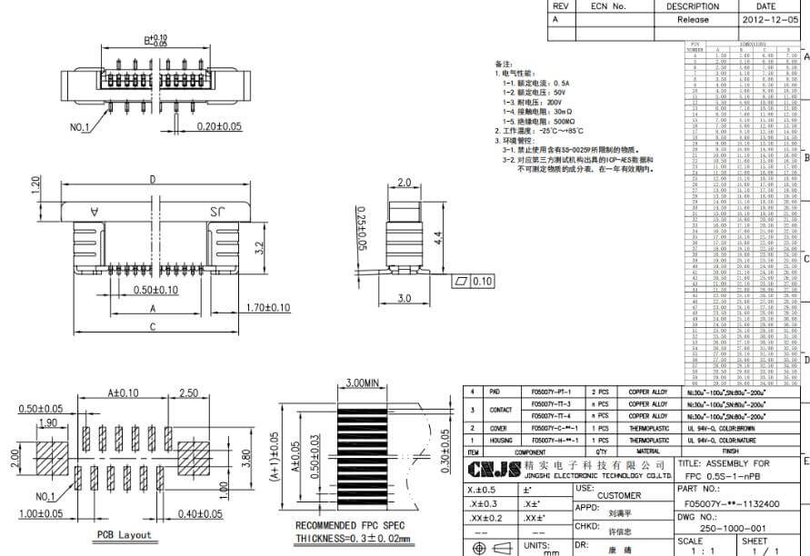
The above are the size parameters of the 60-pin FPC socket and the parameters of the corresponding FPC line.
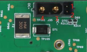
| Serial number | Pin Name | Pin Description | IO level | Remark |
|---|---|---|---|---|
| 1 | I2C_SCL_M3 | Fuel meter I2C interface | 3.3V | This signal is connected to the battery's fuel gauge chip |
| 2 | I2C7_SDA_M3 | 3.3V | ||
| 3 | GND | Signal Ground | 0V | Connecting the rechargeable lithium battery |
| 4 | DC_IN | Battery positive terminal | 12V |
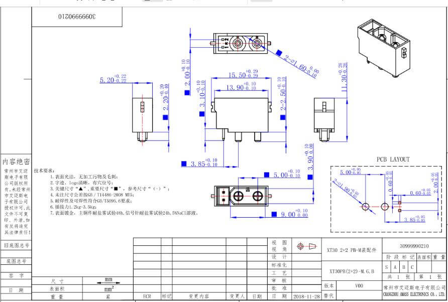
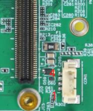
| Serial number | Pin Name | Pin Description | IO level | Remark |
|---|---|---|---|---|
| 1 | GND | Signal Ground | 0V | |
| 2 | FAN_FG | Fan speed feedback signal | 3.3V | This signal can detect the fan speed |
| 3 | VCC5V0_FAN |
Fan power supply |
5V | Fan power supply |
| 4 | FAN_PWM | Fan speed PWM control signal | 5V | The fan speed is controlled by this PWM signal |
This interface is reserved. Whether to add a fan depends on the actual application.
The specifications of the fan socket CON1 are shown in the figure below:
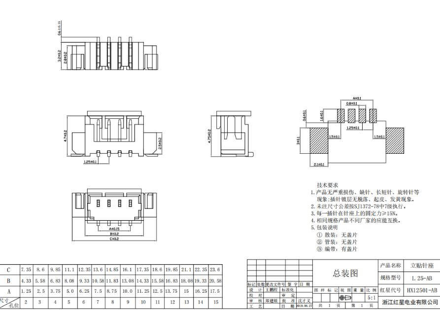
①The pin sequence of the camera interface J20 on the PCBA is shown in the figure below:
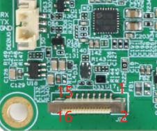
| Serial number | Pin Name | Pin Description | IO level | Remark |
|---|---|---|---|---|
| 1 | GND | Signal Ground | 0V | |
| 2 | USB30_2_SSRXP | USB3.0 HOST receiving signal | ||
| 3 | USB30_2_SSRN | |||
| 4 | GND | Signal Ground | 0V | |
| 5 | USB30_2_SSTXP | USB3.0 HOST sends signal | ||
| 6 | USB30_2_SSTN | |||
| 7 | GND | Signal Ground | 0V | |
| 8 | USB20_HOST0_DP | USB3.0 HOST DP/DM signal | ||
| 9 | USB20_HOST0_DM | |||
| 10 | GND | Signal Ground | 0V | |
| 11 | NC | Dangling | ||
| 12 | NC | |||
| 13 | NC | |||
| 14 | VCC5V0_USB30_HOST1 | USB3.0 HOST power output | 5V | Maximum external output current 900mA |
| 15 | VCC5V0_USB30_HOST1 | 5V | ||
| 16 | VCC5V0_USB30_HOST1 | 5V |
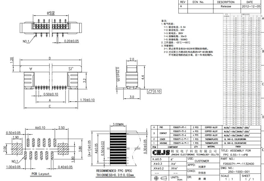
①The pin sequence of the USB interface J18 on the PCBA is shown in the figure below:
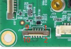
The FPC socket is vertical, and the gold finger contacts of the docked FPC lines should face downwards.
| Serial number | Pin Name | Pin Description | IO level | Remark |
|---|---|---|---|---|
| 1 | GND | Signal Ground | 0V | |
| 2 | TYPEC0_SSTX1P | USB3.0 HOST sends signal | ||
| 3 | TYPEC0_SSTX1N | |||
| 4 | GND | Signal Ground | 0V | |
| 5 | USB30_HOST_DM | USB3.0 HOST DP/DM signal | ||
| 6 | USB30_HOST_DP | |||
| 7 | GND | Signal Ground | 0V | |
| 8 | TYPEC0_SSRX1P | USB3.0 HOST receiving signal | ||
| 9 | TYPEC0_SSRX1N | |||
| 10 | TYPEC0_VBUS5V0 | USB3.0 HOST power output | 5V | Maximum external output current 1000mA |

The above are the size parameters of the 10-pin FPC socket and the parameters of the corresponding FPC line.
Note: The power line (positive and ground line) of the FPC line should be thickened to meet the current requirements. The USB signal line should be made into a differential pair. It is better for the FPC line to have a ground reference plane. It is best to do impedance control. The line sequence should not be punched and crossed, but should be made in a sequential form.
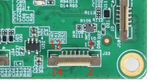
| Serial number | Pin Name | Pin Description | IO level | Remark |
|---|---|---|---|---|
| 1 | FLASH_LIGHT_VCC5V0 | Flash board power output | 5V | Maximum external output current 1580mA |
| 2 | FLASH_LIGHT_VCC5V0 | 5V | ||
| 3 | FLASH_LIGHT_VCC5V0 | 5V | ||
| 4 | FLASH_LIGHT_VCC5V0 | 5V | ||
| 5 | FLASH_LIGHT_VCC5V0 | 5V | ||
| 6 | FLASH_LIGHT_VCC5V0 | 5V | ||
| 7 | SET_PWM | Flash light drive signal | 3.3V | To be connected to the flash board, not controlled by the main board |
| 8 | EN_FLASH | 3.3V | ||
| 9 | GND | Signal Ground | 0V | |
| 10 | GND | Signal Ground | 0V | |
| 11 | GND | Signal Ground | 0V | |
| 12 | GND | Signal Ground | 0V | |
| 13 | GND | Signal Ground | 0V | |
| 14 | GND | Signal Ground | 0V |

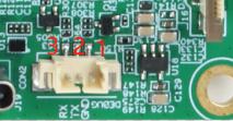
| Serial number | Pin Name | Pin Description | IO level | Remark |
|---|---|---|---|---|
| 1 | GND | Signal Ground | 0V | |
| 2 | DEBUG_TXD | UART sends signal | 3.3V | UART signal is CMOS level |
| 3 | DEBUG_RXD | UART receiving signal | 3.3V |

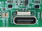
The above is a standard 24-pin Type C interface. This interface can be used as a Type C OTG interface. For connecting a dongle module, it is used as a USB3.0 HOST mode, and the maximum external output current is 1000mA.

The pin sequence of the firmware burning interface J17 on the PCBA is shown in the figure below:
The above is a standard 24-pin Type C interface. However, the USB2.0 signal in Type C is actually used to burn the software program of PCBA.
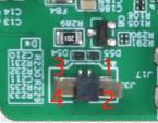
The FPC socket is vertical, and the gold finger contacts of the docked FPC lines should face downwards.
| Serial number | Pin Name | Pin Description | IO level | Remark |
|---|---|---|---|---|
| 1 | BT_LED_K | Bluetooth working status indicator cathode | 5V | The cathode of the LED is connected to the collector of the transistor |
| 2 | BT_LED_K | 5V | ||
| 3 | BT_LED_A | Bluetooth working status indicator anode |
5V | The LED anode is connected to a 5V power supply and a 200 ohm resistor is connected in series. |
| 4 | BT_LED_A | 5V |

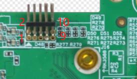
| Serial number | Pin Name | Pin Description | IO level | Remark |
|---|---|---|---|---|
| 1 | SENSOR_VCC3V3 | Sensor 3.3V power supply | 3.3V | |
| 2 | SENSOR_I2C_SCL | Sensor I2C signal | 1.8V | The I2C interface of the six-axis accelerometer and magnetometer shares this signal |
| 3 | SENSOR_1V8 | Sensor 3.3V power supply | 1.8V | |
| 4 | SENSOR_I2C_SDA | Sensor I2C signal | 1.8V | The I2C interface of the six-axis accelerometer and magnetometer shares this signal |
| 5 | GND | Signal Ground | ||
| 6 | COMPASS_nRST | Six-axis acceleration sensor reset signal | 1.8V | Low level is effective |
| 7 | ACCELEROMETER_nINT | Magnetometer sensor interrupt output signal | 1.8V | Falling edge valid |
| 8 | COMPASS_nINT | Six-axis acceleration sensor interrupt output signal | 1.8V | Falling edge valid |
| 9 | GND | Signal Ground | 0V | |
| 10 | GND | Signal Ground | 0V |
Sensor boardSix-axis acceleration sensor chip modelICM-42688, geomagnetic sensor chip model AK09915c.
②Dimensional parameters of double-row pin headers and female headers
The size parameters of the double-row curved pins of J29 on the PCBA are as follows:
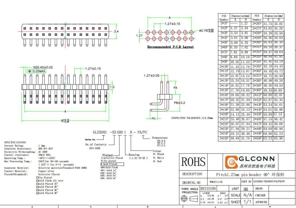
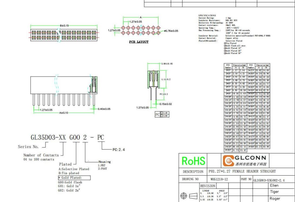
The corresponding size parameters of the double-row female header are shown in the figure below:
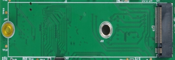
J21 is the connector of M.2 M KEY. PCIE3.0*4Lan, can expand 2280 size solid state drive, with a maximum capacity of 2TB.
J37 is the column supporting the solid-state drive. The size of the column is M3*2.5mm, and the corresponding fixing screw size can be M3*5.0mm.

①Power button
In shutdown state, press the power button for 20ms and the main control will turn on. If in power-on state, press the power button to send a short press or long press interrupt to the main control. If the pull-down time exceeds 6S, it will be forced to shut down (6S, 8S, 10S, 12S software selectable).
②RECOVERY button
Press the RECOVERY button, the system enters the RECOVERY state, under the premise that no button action is performed and the system has been burned with firmware, power on and enter the system directly; if the RECOVERY mode button is pressed when the system starts, RK3588 enters the Loader burning mode, when the PC recognizes the USB device, release the RECOVERY button to burn the firmware.
③Hard reset button
The hard reset button signal is connected to the hardware reset pin of the core board. Press this button and the core board will reset and restart.
④MASKROM button
MASKROM is a dedicated pin for BOOT configuration, which determines the system startup sequence. This pin cannot be used for other functions. Press the MASKROM button, power on the core board again or press the reset button to put the device into the MASKROM state.
| Serial number | name | color | state | Remark |
|---|---|---|---|---|
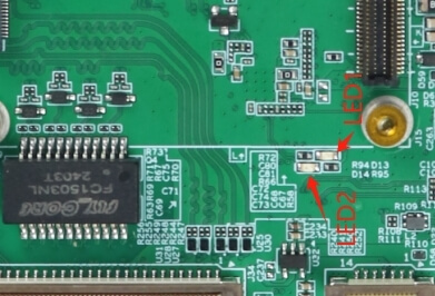
| 1 | LED1 | green | Light = Link up at 100Mbps Blinking = Transiting or Receiving |
The corresponding position number on the PCBA is D13 |
| 2 | LED2 | yellow | Light = Link up at 1000Mbps Blinking = Transiting or Receiving |
The corresponding position number on the PCBA is D14 |
The flashing frequency can be configured through ext Reg0xA00F.
Bit3:0 Flashing frequency:
0000——2Hz;
0101——4Hz;
1010——8Hz;
1111——16Hz.
Bit6:4 Flashing duty cycle (On: Off):
000: 50% ON and 50% OFF;
001: 67% ON and 33% OFF;
010: 75% ON and 25% OFF;
011: 83% ON and 17% OFF;
100: 50% ON and 50% OFF;
101: 33% ON and 67% OFF;
110: 25% ON and 75% OFF;
111: 17% ON and 83% OFF.
4. Software Instructions
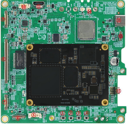
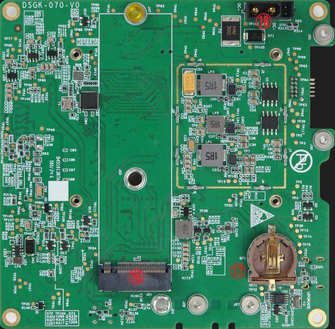
| Serial number | interface | illustrate |
|---|---|---|
| 1 | power button | Sleep/Wake button |
| 2 | loader button | |
| 3 | Reset button | |
| 4 | maskrom key |
| Serial number | interface | illustrate |
|---|---|---|
| 5 | Fan connector | |
| 6 | 3.0 USB interface | |
| 7 | Flash board interface | bypass |
| 8 | 60pin adapter | Transfer LCD, Ethernet port, wifi LED indicator |
| 9 | USB camera interface | |
| 10 | Debug serial port | TTL 3v3 |
| 11 | TypeC dongle interface | |
| 12 | TypeC firmware burning port | The same channel as the 3.0 U disk interface. After the kernel is started, it is configured as a 3.0 host and switched to the U disk interface. |
| 13 | Sensor interface | External compass board |
| 14 | Bluetooth wifi antenna | |
| 15 | Bluetooth LED | |
| 16 | PCIE solid state drive interface | |
| 17 | RTC battery interface | |
| 18 | Power interface |
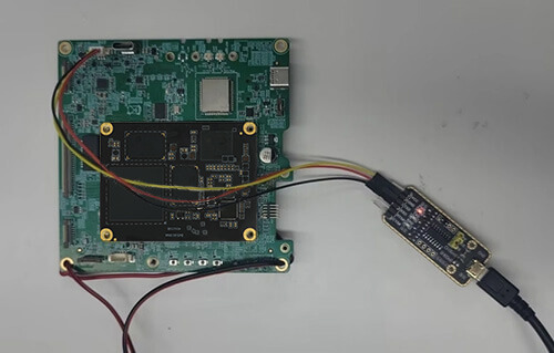
It is recommended to use MobaXterm to access, the recommended download address is: https://mobaxterm.mobatek.net/ download-home-edition.html
The effect after the tool opens the serial port is as follows:
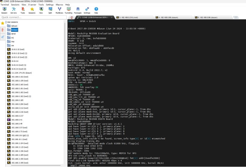
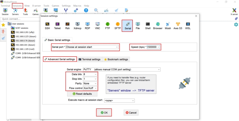
l Debug serial port baud rate 1500000
18 data bits
1 stop bit
No verification
No flow control
Please note that there is no 1500000 in the serial port baud rate drop-down box. You need to enter it directly.
See the figure below for details
| Prepare the Materials | illustrate |
|---|---|
| Burning PC | Windows 7 and above |
| RKDevTool | v2.93 and above |
| USB type C cable |
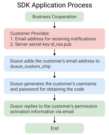
The SDK versions of different Dusun chip platforms need to be applied to the corresponding business end respectively. For example, your company has received the SDK for RK3288, and now there is a new project that requires the SDK for RK3588. We need to contact the corresponding business end of Dusun for business confirmation, and the business end will assist in the application. After approval by Dusun auditors, the technical department can disclose information to your company.
Notice:
The SDK code management released by Dusun follows Google’s REPO method. Users are not recommended to delete the SDK’s REPO and GIT version records.
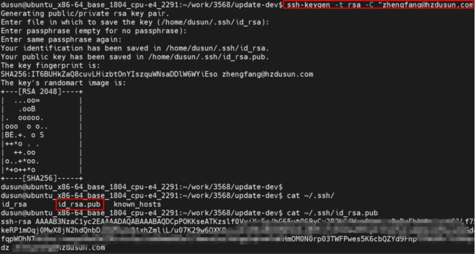
Enter on the server command line
ssh-keygen -t rsa -C " xxxx@xxxx.com "
Keep pressing Enter and do not enter the task characters;
After generating the key, email the ~/.ssh/id_rsa.pub file to Dusun
					git config --global user.email " You@example.com "
git config --global user.name "Your Name"
git clone ssh:// git@roombanker.x3322.net :2223/dusun_repo.git
					sudo cp -f ~/work/dusun_repo/repo /usr/bin/repo
sudo chmod +x /usr/bin/repo
Get the code Please note that each document should modify the repo init address to the corresponding project.
					mkdir -p ~/work/project/dev
cd ~/work/project/dev
repo init -u ssh:// git@roombanker.x3322.net :2223/xxxx
repo sync -c -j8
repo start master --all
Flashing tool link: Baidu Netdisk please enter the extraction code Extraction code: d50y
The computer needs to install the adb USB driver: Baidu Netdisk please enter the extraction code Extraction code: hka6
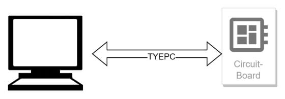
1. One end of the USB data cable is connected to the host, and the other end of the Type-C cable is connected to the firmware burning port of the device.
2. Power on the device
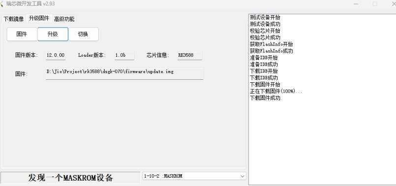
3. Press and hold the maskrom or loader button, then short press the reset button for 1 second and release it, the device enters the maskrom mode or loader mode (the core board in loader mode must be burned with firmware before entering)
Open RKDevTool_Release_v2.93 flashing tool, click Firmware, and select Upgrade Firmware
- Hardware Environment
- Hard disk: 500G or more
- Memory: 16G or more
- Software environment: It is recommended to use the distribution version Ubuntu 20.04
- Update the packages that the compilation depends on
					sudo apt-get update
sudo apt-get install build-essentil flex bison libssl-dev libncurses5
					#Enter the SDK directory
cd RK3588_ANDROID12.0_SDK_070_RELEASE_XXX
# Initialize the compilation environment
source build/envsetup.sh
#Choose the platform you need to compile
lunch rk3588_ds070-userdebug
#One-click compilation
./build.sh -AUCKu
					./build.sh -UCKAu
(WHERE: -U = build uboot
       -C = build kernel with Clang
       -K = build kernel
       -A = build android
       -p = will build packaging in IMAGE
       -o = build OTA package
       -u = build update.img
       -v = build android with 'user' or 'userdebug'
       -d = huild kernel dts name
       -V = build version
       -J = build jobs
   ------------Can be used as needed------------------
)
					rockdev/Image-rk3588_ds070/
├── boot-debug.img
├── boot.img
├── config.cfg
├── dtbo.img
├── MiniLoaderAll.bin
├── misc.img
├── parameter.txt
├── pcba_small_misc.img
├── pcba_whole_misc.img
├── recovery.img
├── resource.img
├── super.img
├── uboot.img
├── update.img
           └── vbmeta.img
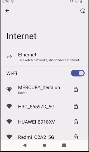
Plug in the network cable, enter the Android system, select Ethernet, and view the Ethernet information.

					EnterMachine command: adb shell
Switch rootCommand: su
					#Turn on wifiled
echo 1 > /sys/class/leds/wifi_led/brightness
Turn off wifiled
echo 0 > /sys/class/leds/wifi_led/brightness
					Turn on the Bluetooth LED
echo 1 > /sys/class/leds/bt_led/brightness
Turn off bluetooth led
echo 0 > /sys/class/leds/bt_led/brightness
Connect the speakers, install NetEase Cloud Music or other music player software, and play songs.

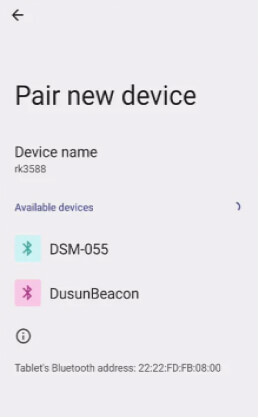
Enter adb shell, enter hwclock to view the rtc time su ; hwclock

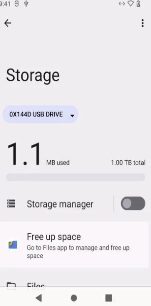
Enter the Android system, Settings->Storage, you can view the SSD information③
③: The solid state drive needs to be formatted in the system when used for the first time.
In the resource manager, you can see that there is an additional USB folder, which is the solid-state drive that has just been added.

| temperature | Fan position |
|---|---|
| <50 | closure |
| 50~55 | 1 |
| 55~60 | 2 |
| 60~65 | 3 |
| 65~70 | 4 |
| >70 | 5 |
					# Check CPU temperature
cat /sys/class/thermal/thermal_zone*/temp
#If the temperature exceeds different ranges, the fan enters different gears
#Fan sys directory path
/sys/devices/platform/pwm-fan/hwmon/hwmon12/
5. Relevant standards and certifications
Chinese Standard: GB/T 26572-2011
EU Standard: Directive 2011/65/EU
Remark:The components used in current products comply with ROHS standards
EU Standard: EU Regulation (EC) No 1907/2006 (REACH)
Remark:The components used in the current products comply with REACH standards
EU standards: EN55032:2015+ A11:2020/EN55035:2017 + A11:2020/ETSI EN 301489-1 V2.2.3(2019-11)/ETSI EN 301489-X
Chinese Standard: GB/T 17625
Remark:Current products are designed strictly in accordance with EMC standards
The customer only needs to provide the application company information, and Dusun will be responsible for all the certification processes
The certification process is shown in the following example (CE certification):
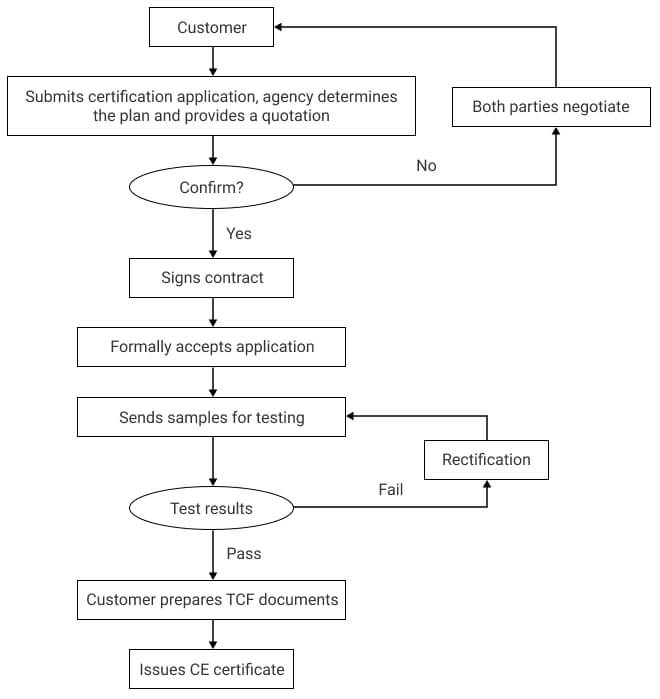
① Dusun provides certification related materials, the list of materials is as follows (contact the project leader, who will coordinate and organize the materials):
- BOM list (all in English)
- Body Label
- Block diagram
- Parts placement
- PCB layout
- Schematic diagram SCH
- User manual
- Antenna Specifications
- List of key safety components (with safety component certificates, such as relays, fuses, terminal blocks, etc.)
- PCB-UL certificate
② Dusun provides certification technical support (fixed frequency, safety regulations, EMC)
Contact the project leader, who will coordinate with relevant technical personnel to provide technical support
6. Order
Please contact sales if you need customization.

