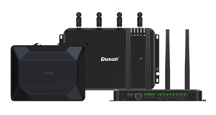
1. DSOM-090M MediaTek MT7621 SOM Introduction
The MT7621 System on Module is equipped with MTK’s MT7621A processor, which includes a dual-core MIPS1004Kc running at a maximum clock speed of 880MHz. Its capabilities make it well-suited for various applications, including Internet service routers, wireless routers, home security gateways, NAS services, and switch control processors.
The MT7621 System on Module is a versatile and powerful platform for developing networking and security solutions. The dual-core architecture enables efficient multitasking and handling of complex network traffic. It can be customized and configured to meet the specific needs of a wide range of applications, from small home networks to large enterprise deployments.
With its robust hardware and advanced features, the MT7621 System on Module is an excellent choice for developers and system integrators looking to build high-performance, reliable, and secure network solutions.
- Size 65mm x 69mm x 2.5mm, featuring sufficient GPIO interfaces
- eMMC up to 8GB
- RAM up to 512MB
- SPI FLASH up to 64MB
- Supports OpenWRT OS
- Supports wireless LAN standards: IEEE 802.11 a/b/g/n/ac
- Frequency range: 2.4GHz~2.4835GHz or 5.18GHz~5.825GHz
- Wireless rate: 300Mbps for 2.4GHz~2.4835GHz frequency range and 866.7Mbps for 5.18GHz~5.825GHz frequency range
- The operating temperature range of the core module is 0~55 degrees
- ROHS certified
- The product is stable and reliable and will operate normally through repeated High/Low Temperature Testing and Restarts Testing.
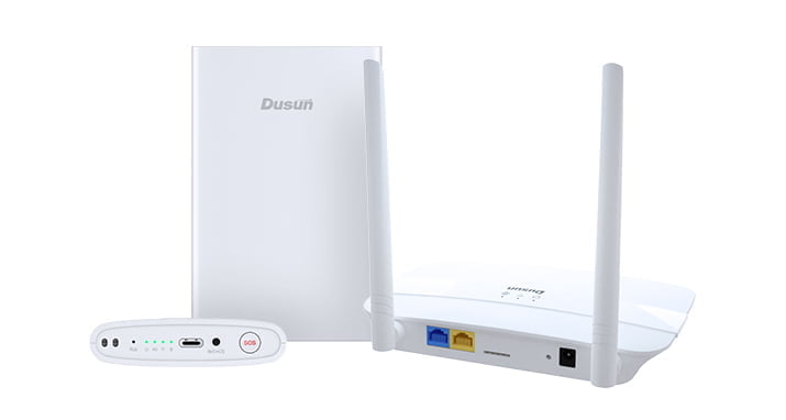
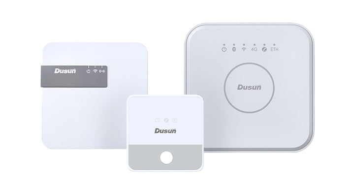
- Routers
- NAS Devices
- iNICs (Intelligent Network Interface Cards)
- Dual Band Concurrent Band
- Home Security Gateway
2. Main chip block diagram of DSOM-090M MediaTek MT7621 SOM


3. Basic Parameters and Interfaces of DSOM-090M MediaTek MT7621 SOM
| Item | Parameter |
|---|---|
| CPU | MIPS 1004Kc(800MHz), I-Cache, D-Cache 32KB, 32KB, L2 Cache 256KB |
| RAM | DDR3L 512MB (128MB, 256MB optional) |
| Memory | eMMC 8GB( 4GB, 16GB optional) |
| Wireless Standard | IEEE 802.11 a/b/g/n/ac |
| Operating Frequency | 2.4 GHz ~ 2.4835 GHz or 5.18GHz ~ 5.825GHz |
| Modulation | IEEE 802.11b: CCK, DQPSK, DBPSK 80211g/a: 64-QAM,16-QAM, QPSK, BPSK 802.11n: 64-QAM,16-QAM, QPSK, BPSK 802.11ac: 256-QAM,64-QAM,16-QAM, QPSK, BPSK |
| Wireless Transmit Rate | 802.11b: 1,2,5.5,11Mbps 802.11g: 6, 9, 12, 18, 24, 36, 48, 54Mbps 802.11n: MCS0~7, HT20 reach up to 72.2Mbps, HT40 reaches up to 150Mbps, HT40 reach up to 300Mbps (2T2R) 802.11ac: VHT20 reach up to 173.3Mbps, VHT40 reach up to 400Mbps VHT80 reaches up to 866.7Mbps |
| Wireless Encryption | WEP/ TKIP/ WPA/ WPA2 |
| Operation Voltage | DC12V/1.5 ( Recommend) |
| OS | OpenWRT |
| Temperature | Operating Temperature: 0° C ~85 °C |
| Storage Temperature: -40 °C ~85 °C | |
| Humidity | 10~90%(Non-condensing) |
| Barometric Pressure | 76Kpa ~ 106Kpa |
| Size | 38mm × 38mm |
| PCB Dimension | 65mm x 69mm x 2.5mm |
| Item | Parameter |
|---|---|
| Audio | 1 x PCM, 1 x I2S |
| eMMC | The onboard interface for eMMC is exposed through pins but should be left unconnected (floating) when not used externally. |
| Ethernet | 4 x GEPHY, 1 x RGMII |
| USB2.0 | 1 x USB 2.0 |
| USB3.0 | 1 x USB 3.0 |
| UART | 3 x UART (UART for Debugging, UART2,a nd UART3 supports Flow Control ) |
| I2C | 1 x I2C |
| JTAG | 1 x JTAG |
| MDC/MDIO | 1 x MDC/MDIO |
| LED Control | Six LED control pins in total: four for the GEPHY interfaces and two to indicate the operating status of the 2.4GHz and 5GHz modes of the Wi-Fi connection. |
4. Pin Definition of DSOM-090M MediaTek MT7621 SOM

| Pin | Name | Type I | I/O Def | I/O | I/O Driv. (mA) | I/O Voltage(V) | Functions |
|---|---|---|---|---|---|---|---|
| 1 | JTMS/GPIO15 | I/O | I | down | 4 | 3.3 | JTAG Mode Select OR GPIO 15 |
| 2 | JTDI/ GPIO14 | I/O | I | down | 4 | 3.3 | JTAG Data Input OR GPIO 14 |
| 3 | JTRST_N/ GPIO17 | I/O | I | down | 4 | 3.3 | JTAG Target Reset OR GPIO 17 |
| 4 | JTDO/ GPIO13 | I/O | O | down | 4 | 3.3 | JTAG Data Output OR GPIO 13 |
| 5 | JTCLK/ GPIO16 | I/O | I | down | 4 | 3.3 | JTAG Clock OR GPIO 16 |
| 6 | LED_WLAN_2.4G | I/O | O | down | 14 | 3.3 | WIFI 2.4GHz status LED indicators |
| 7 | LED_WLAN_5G | I/O | O | up | 16 | 3.3 | WIFI 5GHz status LED indicators |
| 8 | ESW_P3_LED_0 | I/O | I | N/A | 4 | 3.3 | Port 3 PHY LED indicators |
| 9 | ESW_P0_LED_0 | I/O | I | N/A | 4 | 3.3 | Port 0 PHY LED indicators |
| 10 | ESW_P1_LED_0 | I/O | I | N/A | 4 | 3.3 | Port 1 PHY LED indicators |
| 11 | ESW_P2_LED_0 | I/O | I | N/A | 4 | 3.3 | Port 2 PHY LED indicators |
| 12 | D2DB_PORST_N | I | I | N/A | 4 | 3.3 | Power on reset |
| ... | ... | ... | ... | ... | ... | ... | ... |
NOTE:
I/O Types: I = digital-input, O = digital-output, I/O = digital input/output (bidirectional)
A=Analog IO, P = power supply, Def default IO direction for digital IO
All GPIO pins support interrupts.
5. Electrical Parameters of DSOM-090M MediaTek MT7621 SOM
| Parameter | Description | Min | Max | Unit |
|---|---|---|---|---|
| VCC12V0_SYS | VCC12V0_SYS Input voltage | -0.3 | 12.6 | V |
| Ta | Operating temperature range | 0 | 55 | ℃ |
| Ts | Store temperature range | -40 | 85 | ℃ |
Note: Exposure to conditions beyond the absolute maximum ratings may cause permanent damage and affect the reliability and safety of the device and its systems. The functional operations cannot be guaranteed beyond specified values in the recommended conditions.
| Parameter | Description | Min | Typ | Max | Unit |
|---|---|---|---|---|---|
| VCC12V0_SYS | VCC12V0_SYS Input voltage | 11.4 | 12 | 12.6 | V |
| VCC5V0_SYS Supply Current | VCC5V0_SYS Input current | 1.25 | 1.5 | A | |
| Ta | Operating temperature range | 0 | 25 | 55 | ℃ |
| Ts | Store temperature range | -40 | 25 | 85 | ℃ |
6. RF-Performance of DSOM-090M MediaTek MT7621 SOM
| Mode | Rate (Mbps) |
Power(dBm) +1.5dBm | EVM(dB) +2dB | Sensitivity(dBm) +2dBm | ||||||
|---|---|---|---|---|---|---|---|---|---|---|
| CH1 | CH7 | CH13 | CH1 | CH7 | CH13 | CH1 | CH7 | CH13 | ||
| 11b | 1 | 17.5 | 17.5 | 17.5 | -24.5 | -24.5 | -24.5 | -96 | -96 | -96 |
| 11 | 17.5 | 17.5 | 17.5 | -23.2 | -23.2 | -23.2 | -85 | -85 | -85 | |
| 11g | 9 | 17.5 | 17.5 | 17.5 | -30.8 | -30.8 | -30.8 | -87 | -87 | -87 |
| 54 | 17.5 | 17.5 | 17.5 | -31 | -31 | -31 | -69 | -69 | -69 | |
| Mode | Rate (Mbps) |
Power(dBm) +1.5dBm | EVM(dB) +2dB | Sensitivity(dBm) +2dBm | ||||||
| CH3 | CH7 | CH11 | CH3 | CH7 | CH11 | CH3 | CH7 | CH11 | ||
| 11n HT40 |
MCS0 | 14.5 | 14.5 | 14.5 | -31.2 | -31.2 | -31.2 | -87 | -87 | -87 |
| MCS7 | 14.5 | 14.5 | 14.5 | -30.8 | -30.8 | -30.8 | -68 | -68 | -68 | |
| Mode | Rate (Mbps) |
Power(dBm) ±1.5dBm | EVM(dB) ±2dB | Sensitivity(dBm) ±2dBm | |||||||||
|---|---|---|---|---|---|---|---|---|---|---|---|---|---|
| CH36 | CH 100 |
CH 140 |
CH 161 |
CH36 | CH 100 |
CH 140 |
CH 161 |
CH 36 |
CH 100 |
CH 140 |
CH 161 |
||
| 11a | 9 | 18.2 | 18.2 | 18.2 | 18.2 | -31 | -31 | -31 | -31 | -89 | -89 | -89 | -89 |
| 54 | 18.2 | 18.2 | 18.2 | 18.2 | -31 | -31 | -31 | -31 | -73 | -73 | -73 | -73 | |
| Mode | Rate (Mbps) |
Power(dBm) ±1.5dBm | EVM(dB) ±2dB | Sensitivity(dBm) ±2dBm | |||||||||
| CH38 | CH 102 |
CH 142 |
CH 159 |
CH38 | CH 102 |
CH 142 |
CH 159 |
CH 38 |
CH 102 |
CH 142 |
CH 159 |
||
| 11n HT40 |
MCS0 | 17.5 | 17.5 | -30 | -87 | -87 | -87 | ||||||
| 17.5 | 17.5 | 17.5 | 17.5 | -31 | -31 | -31 | -31 | -69 | -69 | -69 | -69 | ||
| CH 42 |
CH 106 |
CH 138 |
CH 155 |
CH 42 |
CH 106 |
CH 138 |
CH 155 |
CH 42 |
CH 106 |
CH 138 |
CH 155 |
||
| 11ac | MCS0 | 16.5 | 16.5 | 16.5 | 16.5 | -30.5 | -30.5 | -30.5 | -30.5 | -84 | -84 | -84 | -84 |
| MCS7 | 16.5 | 16.5 | 16.5 | 16.5 | -33.5 | -33.5 | -33.5 | -33.5 | -57 | -57 | -57 | -57 | |
7. Hardware Design Guidelines of DSOM-090M MediaTek MT7621 SOM

The JTAG interface of the MT7621 chip includes the JTMS, JTDI, JTRST_N, JTDO, and JTCLK pins. The JTAG circuit on the MT7621 System on Module is shown in the above diagram. This interface can be used to debug the MT7621 chip with an external JTAG tool, but it is generally not needed. Several pins in the JTAG interface can be used as GPIO.

The MT7621A chip provides three UART interfaces. In addition to UART1, both UART2 and UART3 have flow control functions. All three UART interfaces can be multiplexed as GPIO, but the RXD, TXD, CTS, and RTS pins of UART2 and UART3 can only be used as a whole for either UART or GPIO functions. The UART2 interface can also be multiplexed as a PCM audio interface, and the UART3 interface can also be multiplexed as an I2S audio interface.
The TXD1 pin of UART1, TXD2, and RTS2_N pins of UART2 and RTS3_N pin of UART3 on the core board have pull-up/down resistors as mode configuration options during chip startup.
The MT7621A chip has one set of USB 2.0 interfaces and one set of USB 3.0 interfaces. Please note when designing the carrier board:
- USB 2.0 and USB 3.0 interfaces are typically used in Host mode for external
connectivity. - It is recommended to reserve a common mode choke on the signal line to
reduce electromagnetic interference. During debugging, resistors or additional
common mode chokes may be used as needed. - USB 2.0 Board Design and Layout Guidelines
Differential pair intra-pair skew less than 10 mils
Differential pair trace length less than 3 inches
Differential pairs have less than 3 through-holes for layer changes
Differential pair impedance controlled to 90 ohms +/-10%.
Differential pairs are spaced using the 3W rule with other signals - USB 3.0 Board Design and Layout Guidelines
Differential pair intra-pair skew less than 5 mils
Differential pair trace length less than 3 inches
Differential pairs have less than 2 through-holes for layer changes
Differential pair impedance controlled to 90 ohms +/-10%.
Differential pairs are spaced using the 3W rule with other signals
l It is necessary to consider the design of protection circuits on the USB circuit
during the PCB design to meet ESD protection requirements. To avoid the effect
of the protection device on the USB signal and to achieve a good protection
effect, the following principles are recommended for the Coreboard design: - The ESD protection device is recommended to be placed close to the USB
connector port. - The ESD protection device is recommended to be an air 15kV, contact 8kV
device with a response time of less than 1ns. - USB 2.0 has a transmission speed of 480Mbps, so the differential signal is very
sensitive to parasitic capacitance on the line. Therefore, ESD protection devices
with low parasitic capacitance should be selected, with a capacitance of less
than 1pF. - USB 3.0 has a transmission speed of 5Gbps, so the differential signal is very
sensitive to parasitic capacitance on the line. Therefore, ESD protection devices
with low parasitic capacitance should be selected, with a capacitance of less
than 0.4pF. - The 2.2 Ohm resistor in series with the USB signal cannot be modified or
omitted
The MT7621A features two audio interfaces: PCM and I2S. The PCM audio interface is multiplexed with the UART2 interface, while the I2S audio interface is multiplexed with the UART3 interface.
- PCM
The correspondence between the PCM audio interface pins and the UART2 interfacepins is as follows
| Pin For PCM Interface | Pin For UART Interface | Description |
|---|---|---|
| PCM_DTX | RTS_N | PCM data output |
| PCM_DRX | CTS_N | PCM data input |
| PCM_CLK | TXD | The PCM clock, also known as the Pulse Code Modulation clock, can be configured to operate at any clock rate between 256k and 8.192MHz. |
| PCM_FS | RXD | PCM data frame synchronization |
- I2S
The correspondence between the I2S audio interface pins and the UART3 interface
pins is as follows:
| Pin For I2S Interface | Pin For UART3 Interface | Description |
|---|---|---|
| I2S_SD0 | RTS_N | PCM data output |
| I2S_CLK | CTS_N | The I2S clock |
| I2S_WS | TXD | I2S channel selection (bit selection) |
| I2S_SDI | RXD | I2S data frame synchronization |
The MT7621A has an I2C interface with a maximum speed of 100KHz. Please note that the clock and data pins of the I2C interface on the System on Module are not connected to pull-up resistors, so external pull-up resistors are required in the design. The resistance value of the pull-up resistors should be selected based on the speed used.
The MT7621 System on Module has four Gigabit Ethernet PHY interfaces, each with the same function. These interfaces are integrated into the MT7621A chip.
The PCB design guidelines for ESW_TXVP_A_P0, ESW_TXVN_A_P0, ESW_TXVP_B_P0, ESW_TXVN_B_P0, ESW_TXVP_C_P0, ESW_TXVN_C_P0, ESW_TXVP_D_P0 and ESW_TXVN_D_P0 are as follows:
Differential pair trace length less than 3 inches
Differential pairs have less than 2 through-holes for layer changes
Differential pair impedance controlled to 100 ohms +/-10%.
Differential pairs are spaced using the 3W rule with other signals
The MT7621A chip has an RGMII/MII interface. MDC and MDIO are used to configure external Ethernet chips.
Note:
When controlling external/internal PHY, MDC/MDIO cannot be used as GPIO; When the total bandwidth of WAN/LAN reaches 2Gbps, the GPIO function on GE2 cannot be used. Leave the pin floating.
- The Design Guidelines for RGMII/MII interfaces are as follows:
| Item | Design Rules |
|---|---|
| Single-ended trace impedance requirement | 50Ω ± 10% |
| TXD0, TXD1, TXD2, TXD3, TXEN, and TXCLK should have equal length | <120mil |
| RXD0, RXD1, RXD2, RXD3, RXDV, and RXCLK should have equal length | <120mil |
| The total length of PCB traces | <5000mil |
| The gap between RGMII signals | >=2 times the line width |
| The gap between RGMII signals and other signals | >=3 times the line width |
| TXCLK and RXCLK routing requirements | must be grounded throughout, grounded routing interval within 300mil must have ground overa hole |
The MT7621 System on Module supports both 2.4GHz and 5GHz wireless functionality. It can be externally connected to two 2.4GHz antennas and one 5GHz antenna via IPEX sockets. The MT7603 chip is used to implement the 2.4GHz wireless functionality, and the MT7613 chip is used to implement the 5GHz wireless functionality on the core board. Both chips have shielding covers installed on top of them to enhance anti-interference performance and reduce external EMI radiation.
8. Product Dimensions of DSOM-090M MediaTek MT7621 SOM


| Item | Parameter |
|---|---|
| Exterior | Stamp Hole |
| Core Board Size | 65mm*69mm*2.5mm |
| Pin Spacing | 1.2mm |
| Pin Pad Size | 1.6mm*0.8mm |
| Number of Pins | 100 Pins |
| Warpage | less than 0.5 % |
9. The methods of Coreboard Thermal Control
The working environment temperature range for the core board is 0℃ to 55℃, so the maximum temperature inside the enclosure cannot exceed 55 degrees.
The MT7621 System on Module is equipped with a heat sink, and the overall size of the core board with the heat sink is 71.3mm × 65.8mm × 16.3mm. Sufficient heat dissipation holes are reserved in the structure when using the MT7621 core board for product design. The heat dissipation holes should allow air convection to dissipate heat from inside the enclosure. If possible, a fan should be used for better heat dissipation.
10. Production Guide of DSOM-090M MediaTek MT7621 SOM
Select modules that can be SMT or in-line packaged according to the customer’s PCB design scheme. If the board is designed for SMT packaging, use SMT-packaged modules. If the board is designed for in-line assembly, use in-line assembly. Modules must be soldered within 24 hours of unpacking. If not, place them in a dry cabinet with a relative humidity of no more than 10% or re-pack them in a vacuum and record the exposure time (total exposure time must not exceed 168 hours).
Instruments or equipment required for SMT assembly:
- SMT Mounter
- SPI
- Reflow soldering
- Oven temperature tester
- AOI
Instruments or equipment required for baking:
- Cabinet ovens
- Antistatic high-temperature trays
- Antistatic and high-temperature gloves
Moisture-proof bags must be stored at a temperature <40°C and humidity <90% RH. Dry-packed products have a shelf life of 12 months from the date of sealing of the package. Sealed packaging with humidity indicator card.

The vacuum bag is found to be broken before unpacking.
After unpacking, the bag is found to be without a humidity indicator card.
The humidity indicator card reads 10% or more after unpacking, and the color ring turns pink.
Total exposure time after unpacking exceeds 168 hours.
More than 12 months from the date of the first sealed packaging.
Baking parameters are as follows:
Baking temperature: 60°C for reel packs, humidity less than or equal to 5% RH; 125°C for tray packs, humidity less than or equal to 5% RH (high-temperature-resistant trays, not blister packs for tow trays).
Baking time: 48 hours for reel packaging; 12 hours for pallet packaging.
Alarm temperature setting: 65°C for reel packs; 135°C for pallet packs.
After cooling to below 36°C under natural conditions, production can be carried out.
If the exposure time after baking is greater than 168 hours and not used up, bake again.
If the exposure time is more than 168 hours without baking, it is not recommended to use the reflow soldering process to solder this batch of modules. The modules are class 3 moisture-sensitive devices and may become damp when the exposure time is exceeded. This may lead to device failure or poor soldering when high-temperature soldering is carried out.
To ensure product qualification rates, it is recommended to use SPI and AOI test equipment to monitor solder paste printing and placement quality
Please follow the reflow profile for SMT placement with a peak temperature of 245°C. The reflow temperature profile is shown below using the SAC305 alloy solder paste.

Description for graphs of curves.
A: Temperature axis
B: Time axis
C: Alloy liquid phase line temperature: 217-220°C
D: Slope of temperature rise: 1-3°C/s
E: Constant temperature time: 60-120s, constant temperature: 150-200°C
F: Time above liquid phase line: 50-70s
G: Peak temperature: 235-245°C
H: the slope of temperature reduction: 1-4°C/s
Note: The above-recommended curves are based on SAC305 alloy solder paste as
an example. Please set the recommended oven temperature curve for other alloy solder pastes according to the solder paste specification.

| Product Model | RAM | eMMC |
|---|---|---|
| DSOM-090M-I | 512 MB | 4 GB |
| DSOM-090M-J | 512 MB | 8 GB |
Documentations
DusunIoT offers full set of development resources including QUICK START, SDK, Firmware packaging, module firmware, Tools, vairous third party software,etc.